that lasts for 10 ms to 20 ms. Again, this reduces the chance of
any pop or click noise from occurring.
example, if only two parameters are to be sent, then it is neces-
sary to write to only two of the five safeload registers.When the
request safe transfer bit is asserted, only those two registers will
be sent; the other three registers are not sent and can still hold
Note that this shutdown sequence assumes that the part is set
to the fast volume ramp speed (Control Register 2, Bit 9). If the
slow ramp speed is set, the volume may not reach zero before the
part enters shutdown and a click or pop may be heard.
The safeload mechanism is not limited to uploading biquad
coefficients; any set of five values in the parameter RAM may be
updated in the same way.This allows real-time adjustment of the
compressor/limiter, delay, or stereo spreading blocks.
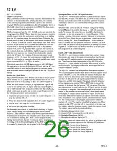
Safeload Mechanism
Many applications require real-time control of filter characteristics,
such as bass/treble controls and parametric or graphic equalization.
To prevent instability from occurring, all of the parameters of a
particular biquad filter must be updated at the same time; other-
wise, the filter could execute for one or two audio frames with a
mixture of old and new coefficients
.
T
his mix of old and new
could cause temporary instability, leading to transients that could
take a long time to decay.
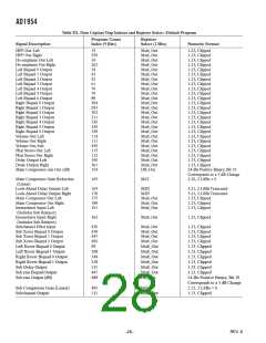
Summary of RAM Modes
TableVII shows the sizes and available modes of the parameter
RAM and the program RAM.
SPI READ/WRITE DATA FORMATS
The read/write formats of the SPI port are designed to be byte-
oriented.This allows for easy programming of common microcon-
troller chips.To fit into a byte-oriented format, 0s are appended
to the data fields to extend the data-word to the next multiple of
8 bits. For example, 22-bit words written to the SPI parameter
RAM are appended with two leading zeroes to reach 24 bits
(3 bytes), and 35-bit words written to the program RAM are
appended with five zeros to reach 40 bits (5 bytes).These zero-
extended data fields are appended to a 2-byte field consisting of a
read/write bit and a 10-bit address.The SPI port knows how many
data bytes to expect based on the address that is received in the
first two bytes.
The method used in the AD1954 to eliminate this problem is to
load a set of five registers in the SPI port with the desired param-
eter RAM address and data. Five registers are used because each
biquad filter has five coefficients. Once these registers are loaded,
the initiate safe transfer bit in Control Register 1 should be set.
Once this bit is set, the processor waits for a period of time in
the program sequence where the parameter RAM is not being
accessed for at least five consecutive instruction cycles.When the
program counter reaches this point, the parameter RAM is writ-
ten with five new data values at addresses corresponding to those
that were entered in the safeload registers.When the operation is
complete, Bit 0 of Control Register 1 (read) is set.This bit may
be polled by the external microprocessor until a 1 is read and
will be reset on a read operation.The polling operation is not
required; the safeload mechanism guarantees that the transfer will
be complete within one audio frame.
The total number of bytes for a single-location SPI write command
can vary from 4 bytes (for a control register write) to 7 bytes (for
a program RAM write). Block writes may be used to fill contiguous
locations in program RAM or parameter RAM.
The read and write formats of the parameter RAM, program RAM
and registers are detailed inTablesVIII to XIX.
The safeload logic automatically sends only those safeload registers
that have been written to since the last safeload operation. For
T
a
bl
e
V
II. Read/Write Modes
Range
Memory
Parameter RAM
256
22 0–255
Direct write, write after core shutdown, safeload write
Direct write, write after core shutdown
Program RAM
TableVIII. Parameter RAM Read/Write Format (Single Address)
Byte 0
Byte 1
Byte 2
Byte 3
Byte 4
Addr[7:0]
00, Param[21:16]
Param[15:8]
Param[7:0]
Table IX. Parameter RAM Block Read/Write Format (Burst Moded)
Byte 5
Byte 6
Byte 7
Byte 8
Byte 9
Byte 10
Byte 0
Byte 1
Byte 2
Byte 3
Byte 4
Addr[7:0]
00, Param[21:16]
Param[15:8]
Param[7:0]
Table X. Program RAM Read/Write Format (Single Address)
Byte 0
Byte 1
Byte 2
Byte 3
Byte 4
Byte 5
Prog[15:8]
Byte 6
Addr[7:0]
00000, Prog[34:32]
Prog[31:24]
Prog[23:16]
Prog[7:0]
REV. A

 ADI [ ADI ]