BRIGHT
Microelectronics
Inc.
BM29F400T/BM29F400B
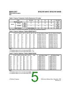
Electronic ID Mode
The Electronic ID mode allows the reading out of a binary code from the device and will identify its
manufacturer and device type. This mode is intended for use by programming equipment for the
purpose of automatically matching the device to be programmed with its corresponding programming
algorithm. This mode is functional over the entire temperature range of the device.
ID
To activate this mode, the programming equipment must force V (11.5V to 12.5V) on address pin
A9. Two identifier bytes may then be sequenced from the device outputs by toggling address A0 from
IL
V
IH
to V . All addresses are don't cares except A0, A1, and A6 (see Table 3).
Manufacturer and device codes may also be read via the command register; for instance, when the
BM29F400 is erased or programmed in a system without access to high voltage on the A9 pin. The
command sequence is illustrated in Table 6 (refer to Electronic ID Command section).
IL
Byte 0 (A0 = V ) represents the manufacturer's code (Bright Microelectronics = ADH) and byte 1 (A0
IH
= V ) the device identifier code (BM29F400T = 23H and BM29F400B = ABH for 8-bit mode;
BM29F400T = 2223H and BM29F400B = 22ABH for 16-bit mode). These two byte words are given in
Table 3. To read the proper device codes when executing the Electronic ID, all identifiers for
manufacturer and device will exhibit odd parity with the MSB (DQ7) defined as the parity bit. A1 must
IL
be V (see Table 3).
Read Mode
The BM29F400 has three control functions which must be satisfied in order to obtain data at the
CE
OE
is the output control
outputs.
is the power control and should be used for device selection.
WE
and should be used to gate data to the output pins if a device is selected. As shown in Table 1,
should be held at V , except in Write mode and Enable Sector Protect mode.
IH
Address access time (tACC) is equal to the delay from stable addresses to valid output data. Chip
CE
OE
enable access time (tCE) is the delay from stable addresses and stable
to valid data at the output
to valid data at the output
pins. Output enable access time is the delay from the falling edge of
-
pins (assuming the addresses have been stable for at least tACC tOE time).
Standby Mode and Hardware RESET Standby Mode
The BM29F400 has two methods for implementing standby mode. The first method requires use of
CE
RESET
RESET
both the
pin and the
pin. The second method only requires use of the
pin.
CE
RESET
When using both pins, a CMOS standby mode is achieved when both
and
are held at
±
m
Vcc 0.5V. In this condition, the current consumed is typically less than 100 A. A TTL standby mode
IH
CE
RESET
held at V . In this condition, the typical current required is
is achieved with both
and
m
reduced to 200 A. The device can be read with standard access time (tCE) from either of these two
standby modes.
SS
RESET
RESET
When using the
pin only, a CMOS standby mode is achieved with
held at V
±
m
0.5V. In this condition, the current consumed is typically less than 100 A. A TTL standby mode is
IL
RESET
achieved with
held at V . In this condition, the typical current required is reduced to 1 mA.
pin is taken high, the device requires 500 nS of wake-up time before outputs are
valid for a read access.
RESET
Once the
- 6 -

 WINBOND [ WINBOND ]