BRIGHT
Microelectronics
Inc.
BM29F400T/BM29F400B
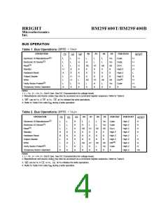
Read RESET Command
RESET
The read or
operation is initiated by writing the Read/Reset command sequence in to the
command register. Microprocessor read cycles retrieve the data from the memory. The device
remains enable for reads until the command register contents are changed.
The device will automatically power-up in the Read/Reset mode. In this case, a command sequence
is not needed to read the memory data. This default power-up to Read mode ensures that no spurious
changes of the data can take place during the power transitions. Refer to the AC Characteristics for
Read-Only Operation and the respective Timing Waveforms for the specific timing parameters.
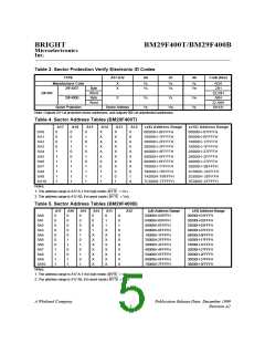
Electronic ID Command
The BM29F400 contains an Electronic ID command to supplement the traditional PROM
programming method described in the Electronic ID Mode section. The operation is initiated by writing
the Electronic ID command sequence into the command register. Following command write, a read
cycle from address XX00H retrieves manufacturer code of ADH. A read cycle from address XX01H
returns the device code (BM29F400T = 23H and BM29F400B = ABH for 8-bit mode; BM29F400T =
2223H and BM29F400B = 22ABH for 16-bit mode) (see Table 3). All manufacturer and device codes
exhibit odd parity with the MSB (DQ7) defined as the parity bit.
The Electronic ID command can also be used to identify protected sectors. After writing the Electronic
ID command sequence, the CPU can scan the sector addresses (see Table 4 and Table 5) while (A6,
A1, A0) = (0, 1, 0). Protected sectors will return 01H on the data outputs and unprotected sectors will
return 00H. To terminate the operation, it is necessary to write the Read/Reset command sequence
into the command register.
Byte/Word Programming Command
The device is programmed on a byte-by-byte (or word-by-word) basis. Programming is a four bus
cycle operation (see Table 6). There are two "unlock" write cycles. These are followed by the program
CE
CE
WE
WE
set-up command and data write cycles. Addresses are latched on the falling edge of
whichever happens later, and program data (PD) is latched on the rising edge of
or
or
,
,
CE
WE
, whichever happens first, begins
whichever happens first. The rising edge of
programming using the Embedded Program Algorithm.
or
Upon executing the algorithm, the system is not required to provide further controls or timings. The
device will automatically provide adequate internally generated program pulses and verify the
programmed cell margin.
The automatic programming operation is completed when the data on DQ7 (also used as Data
Polling) is equivalent to the data written to this bit at which time the device returns to the read mode
and addresses are no longer latched (see Table 7, Write Operation Status Flags). Therefore, the
device requires that a valid address to the device be supplied by the system at this particular instance
Data
Data
Polling must be performed at the memory location which is
of time for
being programmed.
Any commands written to the chip during the Internal Program Algorithm will be ignored. If a
Polling operations.
RESET
hardware
be corrupted.
occurs during the programming operation, the data at that particular location will
- 8 -

 WINBOND [ WINBOND ]