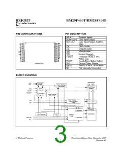
BRIGHT
Microelectronics
Inc.
BM29F400T/BM29F400B
If the device is deselected during programming or erase, the device will draw active current until the
programming or erase operation is completed. In the standby mode the outputs are in a high
OE
impedance state, independent of the
input.
Output Disable Mode
IH
OE
With the
input at a logic high level (V ), output from the device is disabled. This will cause the
IL
IH
CE
WE
= V for
output pins to be in a high impedance state. It is shown in Table 1 that
= V and
Output Disable. This is to differentiate Output Disable mode from Write mode and to prevent
inadvertent writes during Output Disable.
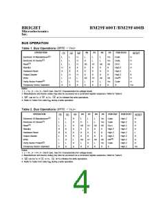
Program and Erase Modes
Device programming and erase are accomplished via the command register. Contents of the register
serve as inputs to the internal state machine. Outputs of the state machine dictate the function of the
device.
The command register itself does not occupy any addressable memory locations. The register is a
latch used to store the commands along with the addresses and data information needed to execute
IL
IL
WE
CE
CE
OE
is
the command. The command register is written by bringing
WE
to V , while
is at V and
IH
at V . Addresses are latched on the falling edge of
or
, whichever happens later, while data
WE CE
is latched on the rising edge of
or
, whichever happens first. Standard microprocessor write
timings are used. Refer to AC Characteristics for Programming/Erase and their respective Timing
Waveforms for specific timing parameters.
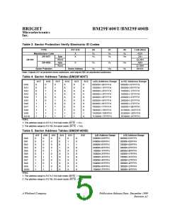
Enable Sector Protect and Verify Sector Protect Modes
The BM29F400 has a hardware Sector Protect mode that disables both Programming and Erase
operation to the protected sector(s). There are total of 11 sectors in this device. The sector protect
feature is enabled using the programming equipment at the user's site. The device is shipped from
the BMI factory with all sectors unprotected.
ID
To verify programming of the protection circuitry, the programming equipment must force V on the
IL
IH
CE
OE
WE
address pin A9 with
and
at V and at V . As shown in Table 2, scanning the sector
addresses while (A6, A1 and A0) = (0, 1, 0) will produce a 01H code at the device output pins for a
protected sector. In the Verify Sector Protect mode, the device will read 00H for an unprotected
sector. In this mode, the lower order addresses, except for A0, A1 and A6, are don't care. Address
IL
locations with A1 = V are reserved for Electronic ID manufacturer and device codes. It is also
possible to determine if a sector is protected in-system by writing the Electronic ID command
(described in the Electronic ID command section below.)
Temporary Sector Unprotect Mode
The BM29F400 has a Temporary Sector Unprotect feature that allows the protect feature to be
temporarily suspended to change data in a protected sector in-system. The Temporary Sector
ID
-
pin to V (11.5V 12.5V).
RESET
Unprotect mode is activated by setting the
In this mode, protected sectors can be programmed or erased by selecting the sector addresses.
ID
RESET
Once V is removed from the
pin, all previously protected sectors will be protected. Refer to
the Temporary Sector Unprotect algorithm and timing waveforms.
A Winbond Company
Publication Release Date: December 1999
Revision A2
- 7 -

 WINBOND [ WINBOND ]