BRIGHT
Microelectronics
Inc.
BM29F400T/BM29F400B
4MEGABIT (512K 8/ 256K 16)
´
´
5VOLT SECTOR ERASE CMOS FLASH MEMORY
GENERAL DESCRIPTION
The BM29F400 is an 4 Megabit, 5.0 volt-only CMOS Flash memory device organized as a 512
Kbytes of 8-bits each, or 256 Kbytes of 16 bits each. The device is offered in standard 48-pin TSOP
package. It is designed to be programmed and erased in-system with a 5.0 volt power-supply and can
also be reprogrammed in standard EPROM programmers.
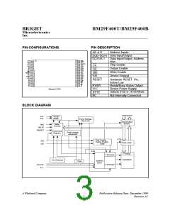
CE
With access times of 90 nS, 120 nS, and 150 nS, the BM29F400 has separate chip enable
, write
WE OE
enable
, and output enable
controls. BMI's memory devices reliably store memory data even
after 100,000 program and erase cycles.
The BM29F400 is entirely pin and command set compatible with the JEDEC standard for 4 Megabit
Flash memory devices. Commands are written to the command register using standard
microprocessor write timings. Register contents serve as input to an internal state-machine which
controls the erase and programming circuitry. Write cycles also internally latch addresses and data
needed for the programming and erase operations.
The BM29F400 is programmed by executing the program command sequence. This will start the
internal byte/word programming algorithm that automatically times the program pulse width and also
verifies the proper cell margin. Erase is accomplished by executing either the sector erase or chip
erase command sequence. This will start the internal erasing algorithm that automatically times the
erase pulse width and also verifies the proper cell margin. No preprogramming is required prior to
execution of the internal erase algorithm. Sectors of the BM29F400 Flash memory array are
electrically erased via Fowler-Nordheim tunneling. Bytes/words are programmed one byte/word at a
time using a hot electron injection mechanism.
The BM29F400 features a sector erase architecture. The device memory array is divided into one 16
Kbytes, two 8 Kbytes, one 32 Kbytes, and seven 64 Kbytes. Sectors can be erased individually or in
groups without affecting the data in other sectors. Multiple sector erase and full chip erase capabilities
add flexibility to altering the data in the device. To protect this data from accidental program and
erase, the device also has a sector protect function. This function hardware write protects the
selected sector(s). The sector protect and sector unprotect features can be enabled in a PROM
programmer.
For read, program and erase operation, the BM29F400 needs a single 5.0 volt power-supply.
Internally generated and well regulated voltages are provided for the program and erase operation. A
low Vcc detector inhibits write operations on loss of power. End of program or erase is detected by the
Ready/Busy status pin, Data Polling of DQ7, or by the Toggle Bit I feature on DQ6. Once the program
or erase cycle has been successfully completed, the device internally resets to the Read mode.
RESET
RESET
pin low during execution of an
The BM29F400 also has a hardware
Internal Programming or Erase command will terminate the operation and reset the device to the
RESET
pin. Driving the
Read mode. The
access to boot code upon completion of system reset, even if the Flash device is in the process of an
RESET
pin may be tied to the system reset circuitry, so that the system will have
Internal Programming or Erase operation. If the device is reset using the
pin during an
Internal Programming or Erase operation, data in the address locations on which the internal state
A Winbond Company
Publication Release Date: December 1999
Revision A2
- 1 -

 WINBOND [ WINBOND ]