BRIGHT
Microelectronics
Inc.
Preliminary BM29F040
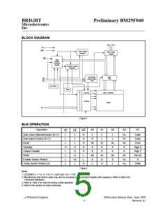
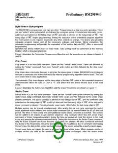
BLOCK DIAGRAM
0
7
DQ - DQ
Vcc
GND
Erase Voltage
Generator
Input / output
Buffers
WE
State
Control
Command
Register
Program Voltage
Generator
Data
latch
Chip Enable
Output Enable
Logic
CE
OE
Vcc Detect
Timer
A
d
d
Y-Decode
Y-MUX / SENSING
r
e
s
s
L
a
t
X-decode
ARRAY
A 0 - A 18
c
h
Figure 1
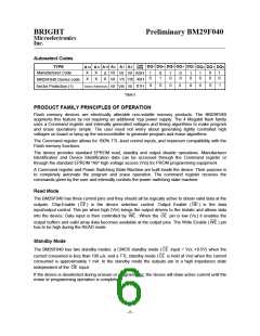
BUS OPERATION
Operation
A0
A1
A6
A9
I/O
WE
H
H
H
X
CE
L
OE
L
Auto select Manufacturers ID (1)
Auto select Device ID (1)
Read
L
H
L
L
L
L
VID
VID
A9
X
Code
Code
Dout
L
L
L
L
A0
X
A1
X
A6
X
Standby
H
L
X
High Z
High Z
Din (2)
X
Output Disable
H
H
VID
L
H
L
X
X
X
X
Write
L
A0
X
A1
X
A6
X
A9
VID
VID
Enable Sector Protect
Verify Sector Protect (3)
L
L
L
H
L
H
L
Code
Table 4
Notes:
1. LEGENDS: L = VIL, H = VIH, X = don't care, VID = +12V.
2. Manufacturer and device codes may also be accessed via a command register write sequence. Refer to table 6 for
Command definitions.
3. Refer to Table 4 for valid Din during a write operation.
4. Refer to the section on sector protection.
A Winbond Company
Publication Release Date: June 1999
Revision A1
- 5 -

 WINBOND [ WINBOND ]