BRIGHT
Microelectronics
Inc.
Preliminary BM29F040
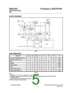
Flexible Sector-erase Architecture:
64K bytes per sector
Individual sector, multiple sector or bulk erase capability.
Individual or multiple-sector protection is user definable.
Table 2. Sector Definition
64K byte sector
64K byte sector
64K byte sector
64K byte sector
64K byte sector
64K byte sector
64K byte sector
64K byte sector
70000H-7FFFFH
60000H-6FFFFH
50000H-5FFFFH
40000H-4FFFFH
30000H-3FFFFH
20000H-2FFFFH
10000H-1FFFFH
00000H-0FFFFH
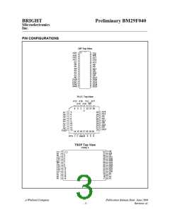
PIN DESCRIPTION
SYMBOL
TYPE
NAME AND FUNCTION
A0 - A18
I
ADDRESS INPUTS: for memory addresses. Addresses are internally
latched during a write cycle.
A9
I
ADDRESS INPUT: When A9 is at 12 Volts the ID mode is accessed. During
this mode A0 decodes between the manufacturer and device ID¢s.
DQ0-DQ7
I/O
DATA INPUTS / OUTPUTS: Inputs array data on the fourth
and WE
CE
cycle during a program command. Inputs commands WE to the Command
register when and WE are active. Data is internally latched during the
CE
program cycles. Outputs are from Array and Intelligent Identifier
information. The output pins float to tri-state when the chip is deselected or
the outputs are disabled.
I
I
CHIP ENABLE: Activates the device's control logic, input buffers, decoders
CE
OE
and sense amplifiers.
is active low control;
high deselects the
CE
CE
memory device and reduces power consumption to standby levels.
OUTPUT ENABLE: is active low control signal. This pin gates the
OE
’ s
device outputs through the data buffers during a read cycle. When
is
CE
low and
is high the outputs are tri-state.
OE
I
WRITE ENABLE: Controls writes to the Command state Machine and
memory array. WE is active low signal. Addresses and Data are latched
during the rising edge of the WE pulse.
WE
Vcc
DEVICE POWER SUPPLY: Main power source to the device. It¢s value is
5V ± 10% or 5V ± 5%.
GND
GROUND: The device ground for the internal circuitry.
Table 3
- 4 -

 WINBOND [ WINBOND ]