TGF2023-10
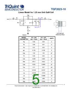
Table III
RF Characterization Table 1/
Bias: Vd = 32 V & 40 V, Idq = 1 A, Vg = - 3V Typical
SYMBOL
PARAMETER
Vd = 40 V
Vd = 32 V
UNITS
Power Tuned:
Psat
PAE
Saturated Output Power
Power Added Efficiency
Power Gain
47.5
46
46.5
47
dBm
%
Gain
15
15
dB
Rp 2/
Parallel Resistance
Parallel Capacitance
Load Reflection Coefficient
87.79
68.58
Ω·mm
pF/mm
-
Cp 2/
0.444
0.461
0.819 ‚107.7
0.831 ‚172.6
ГL 3/
Efficiency Tuned:
Psat
Saturated Output Power
Power Added Efficiency
Power Gain
45
55
44.5
57
dBm
%
PAE
Gain
19.5
19.5
dB
Rp 2/
Parallel Resistance
Parallel Capacitance
Load Reflection Coefficient
190.2
158.1
Ω·mm
pF/mm
-
Cp 2/
0.263
0.314
0.716 ‚157.7
0.753 ‚161.7
ГL 3/
1/
2/
3/
Values in this table are scaled from a 1.25 mm unit GaN on SiC cell at 3.5 GHz
Large signal equivalent GaN on SiC output network
Optimum load impedance for maximum power or maximum PAE at 3.5 GHz. The series resistance
and inductance (Rd and Ld) shown in the Figure on page 5 is excluded
3
TriQuint Semiconductor: www. triquint.com (972)994-8465 Fax (972)994-8504 Info-mmw@tqs.com
Dec 2008 © Rev A

 TRIQUINT [ TRIQUINT SEMICONDUCTOR ]