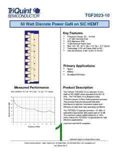
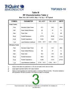
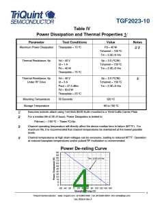
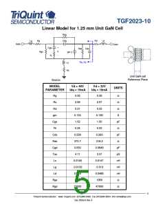
TGF2023-10
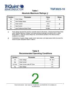
Table I
Absolute Maximum Ratings 1/
Symbol
Parameter
Value
Notes
Vd
Drain Voltage
40 V
-10 to 0 V
10 A
2/
Vg
Id
Gate Voltage Range
Drain Current
2/
2/
Ig
Gate Current
56 mA
35 dBm
Pin
Input Continuous Wave Power
1/
2/
These ratings represent the maximum operable values for this device. Stresses beyond those listed
under “Absolute Maximum Ratings” may cause permanent damage to the device and / or affect
device lifetime. These are stress ratings only, and functional operation of the device at these
conditions is not implied.
Combinations of supply voltage, supply current, input power, and output power shall not exceed the
maximum power dissipation listed in Table IV.
Table II
Recommended Operating Conditions
Symbol
Vd
Parameter
Value
28 - 40 V
1 A
Drain Voltage
Drain Current
Idq
Id_Drive
Vg
Drain Current under RF Drive
Gate Voltage
3 A
-3 V
2
TriQuint Semiconductor: www. triquint.com (972)994-8465 Fax (972)994-8504 Info-mmw@tqs.com
Dec 2008 © Rev A

 TRIQUINT [ TRIQUINT SEMICONDUCTOR ]