OX9162
OXFORD SEMICONDUCTOR LTD.
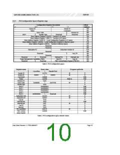
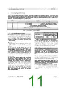
Mode
Dir1
Name
Description
Parallel
Multi-purpose & External interrupt pins
104, 65 I/O
Local Bus
MIO[1:0]
Multi-purpose I/O pins. Can drive high or low, or assert a PCI
interrupt
EEPROM pins
98
94
96
O
O
IU
EE_CK
EE_CS
EE_DI
EEPROM clock
EEPROM active-high Chip Select
EEPROM data in. When the serial EEPROM is connected,
this pin should be pulled up using 1-10k resistor. When the
EEPROM is not used the internal pull-up is sufficient.
EEPROM data out.
95
Miscellaneous pins
107
O
EE_DO
ID
I
MODE
TEST
Mode selection: Parallel Port (0) or Local Bus (1)
Test Pin : should be held low at all times
93
Power and ground2
9, 31, 47, 70, 124
17, 54, 81, 113
V
V
AC VDD
DC VDD
Supplies power to output buffers in switching (AC) state
Power supply. Supplies power to core logic, input buffers
and output buffers in steady state
4, 8, 21, 30, 40, 48, 57,
69, 75, 86, 119, 123
16, 53, 80, 111
G
G
AC GND
DC GND
Supplies GND to output buffers in switching (AC) state
Ground (0 volts). Supplies GND to core logic, input buffers
and output buffers in steady state
Table 1: Pin Descriptions
Note 1: Direction key:
I
Input
P_I
PCI input
ID
O
Input with internal pull-down
Output
P_O
P_I/O
PCI output
PCI bi-directional
I/O
OD
NC
Z
Bi-directional
Open drain
No connect
P_OD PCI open drain
G
V
Ground
5.0V power
High impedance
Note 2: Power & Ground
There are two GND and two VDD rails internally. One set of rails supply power and ground to output buffers while in switching
state (called AC power) and another rail supply the core logic, input buffers and output buffers in steady-state (called DC rail).
The rails are not connected internally. This precaution reduces the effects of simultaneous switching outputs and undesirable RF
radiation from the chip. Further precaution is taken by segmenting the GND and VDD AC rails to isolate the PCI and Local Bus
pins.
Data Sheet Revision 1.1 PRELIMINARY
Page 7

 OXFORD [ OXFORD SEMICONDUCTOR ]