FEDL87V2107-01
OKI Semiconductor
ML87V2107
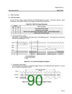
•
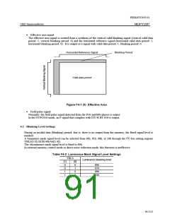
Effective area signal
The effective area signal is created from a synthesis of the vertical valid blanking signal (vertical valid data
period: 1, vertical blanking period: 0) and the horizontal reference signal (horizontal valid data period: 1,
horizontal blanking period: 0). It is output as a signal with valid data period: 1, blanking period: 0.
Horizontal Reference Signal
Blanking Period
Valid data period
Figure F4-1 (3) Effective Area
•
Field pulse signal
Normally, the field pulse signal detected from the IVS and IHS phases is output.
In the SYNC656 mode, an F signal that complies with ITU-R BT.656 is output.
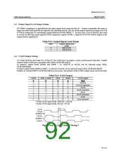
4.2 Blanking Level Settings
During an invalid data (blanking) period, that is, there is no output from the memory, the fixed signal level is
masked.
A luminance mask signal level can be selected from 00h, 01h, 08h, or 10h through the I2C-bus setting register
YBLS[1:0] (SUB:40h-bit[5:4]).
The chrominance mask signal level is fixed to 80h.
In external memory control mode or direct noise reduction mode, this function is ineffective.
Table F4-2 Luminance Mask Signal Level Settings
YBLS
Luminance blanking level
[1]
0
[0]
0
00h
01h
08h
10h
0
1
1
0
1
1
91/152

 OKI [ OKI ELECTRONIC COMPONETS ]