FEDL87V2107-01
OKI Semiconductor
ML87V2107
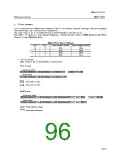
4.3 Output Signal Level Range Settings
ITU-R601 compliance is specified for the input signal level range for this IC. Output is normally the same as
input, but where 00h and FFh are input for the valid data period, you can set the output signal level range to be 01h
to FEh by setting the I2C-bussettings register R601(SUB:40h-bit[6]) = 1. In such cases, even if YBLS[1:0] is used
to set the invalid data mask signal level for luminance signals to 00h, a signal level of 01h will be output as the
output lowest signal level.
Table F4-3 Output Signal Level Range
R601
Output signal level
range
0
1
00h to FFh
01h to FEh
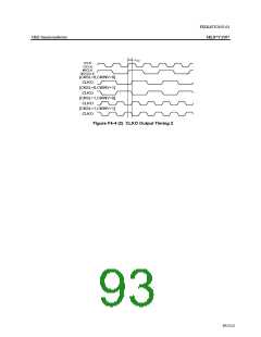
4.4 CLKO Output Setting
As a data latch for post-stage ICs of this IC, the CLKO pin can output a clock synchronized with data. Enable
control of the CLKO pin is possible with CKEN (SUB:60h-bit[7]).
In memory output mode (IDNR and IDNR = 0), OOCLK or OCLK can be selected using CKSL
(SUB:60h-bit[6]).
In direct output mode (DNR or DNR = 1), IICLK or ICLK can be selected using CKSL (SUB:60h-bit[6]).
Further, by setting CKINV (SUB:60h-bit[5]) as necessary, the polarity of the CLKO output clock can be inverted.
Table F2-4 CLKO Output
CKEN
DNR or IDNR
CKSL
CKINV
CLKO output
Hi-Z
0
1
1
1
1
1
1
1
1
0
0
0
0
0
1
1
1
1
X
0
0
1
1
0
0
1
1
X
0
1
0
1
0
1
0
1
OOCLK
OOCLK inversion
OCLK
OCLK inversion
IICLK
IICLK inversion
ICLK
ICLK inversion
* In the 16-bit input mode, OOCLK = OCLK.
* In the 16-bit input mode, IICLK = ICLK.
tCKD
ICLK
OCLK
[CKINV=0]
CLKO
[CKINV=1]
CLKO
Figure F4-4 (1) CLKO Output Timing 1
92/152

 OKI [ OKI ELECTRONIC COMPONETS ]