FEDL87V2107-01
OKI Semiconductor
ML87V2107
3. Sync. Signal Generation
3.1 Sync. Signal Generation for Output
This IC can generate vertical and horizontal Sync. signals for output processing. As a result, control on the output
side is enabled without an external Sync. signal generator.
3.1.1 Sync. Signal Generation Mode Settings
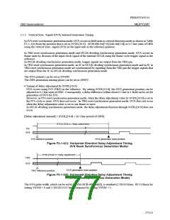
In this IC, a Sync. signal generation mode is set by setting the external setting pins (ASYNC, INT) or the internal
registers (IAYSINC, IINT).
A Sync. signal generation mode can be selected from the IVS reset synchronous generation mode, TRG reset
synchronous generation mode, and OCLK-dividing synchronous generation mode.
In IVS reset generation synchronous mode, the field phase can also be set by setting SFINV.
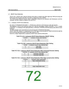
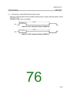
Table F3-1-1(4) lists the options available for the Sync. signal timing of this IC.
Table F3-1-1(1) OHS and OVS Generation Mode Setting
ASYNC or
IASYNC
INT or
IINT
OHS and OVS generation mode setting
Internal synchronous generation stop mode (external
synchronous frame buffer output)
0
0
0
1
IVS reset synchronous generation mode (Input vertical
synchronous frame buffer output)
TRG reset synchronous generation mode
(Frame-trigger- vertical synchronous frame buffer
output)
1
1
0
1
OCLK-dividing synchronous generation mode
(Asynchronous frame buffer output)
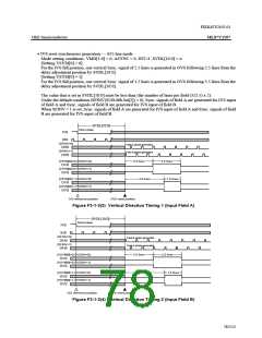
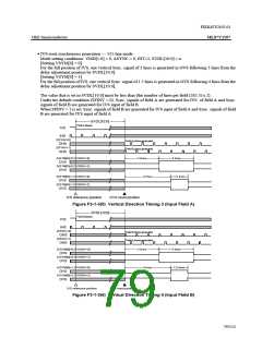
Table F3-1-1(2) Generation Field Setting (in IVS Reset Generation Mode)
Mode
Input field
SFINV Generation field
0
1
0
1
A
B
B
A
A
Normal
B
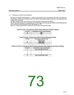
Table F3-1-1(4) Normal Mode Synchronous Generation Timing Setting
VMD
HMD
IICLK
OOCLK
Number of
pixels per
line
Horizontal
mode
Frequency
(MHz)
Frequency
(MHz)
[1]
[0]
[1]
[0]
0
0
0
0
0
0
0
1
0
1
0
1
0
0
0
0
1
1
0
0
1
1
0
0
13.5
13.5
13.5
13.5
625/50Hz 2:1
525/60Hz 2:1
625/50Hz 2:1
525/60Hz 2:1
625/50Hz 2:1
525/60Hz 2:1
864
858
944
780
944
910
14.75
14.75
12.272727
14.75
12.272727
14.75
14.31818
14.31818
Others
Test mode (not settable)
*: IICLK is the input internal sampling clock.
*: OOCLK is the output internal sampling clock.
75/152

 OKI [ OKI ELECTRONIC COMPONETS ]