EM785830AA
8-bit Micro-controller
PAGE1 (Unused)
7
0
6
0
5
0
4
0
3
0
2
0
1
0
0
0
R/W-0
R/W-0
R/W-0
R/W-0
R/W-0
R/W-0
R/W-0
R/W-0
** This page must clear to 0 or the power consumption of MCU will increase.
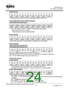
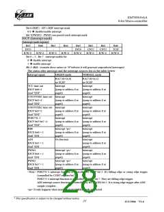
IOC9 (PORT9 I/O control, PORT9 switches)
PAGE0 (PORT9 I/O control register)
7
6
5
4
3
2
1
0
IOC97
R/W-1
IOC96
R/W-1
IOC95
R/W-1
IOC94
R/W-1
IOC93
R/W-1
IOC92
R/W-1
IOC91
R/W-1
IOC90
R/W-1
Bit 0 ~ Bit 7 (IOC90 ~ IOC97) : PORT9(0~7) I/O direction control register
0 Î put the relative I/O pin as output
1 Î put the relative I/O pin into high impedance
PAGE1 (Unused)
7
0
6
0
5
0
4
0
3
0
2
0
1
0
0
0
R/W-0
R/W-0
R/W-0
R/W-0
R/W-0
R/W-0
R/W-0
R/W-0
**These 8 bits must clear to 0 or Port9 input or output function will wronging
IOCA (Unused)
PAGE0(undefined) not allowed to use
PAGE1(undefined) not allowed to use
7
X
-
6
0
5
X
-
4
X
-
3
0
2
X
-
1
0
0
0
R/W
R/W
R/W-0
R/W-0
Bit0~Bit1 : Undefined registers. Please clear these two bits to 0.
Bit3 , Bit6 (Unused) : These 2 bits must clear to 0 or MCU power consumption will increase.
Bit2, 4,5,6 are undefined register, they are not allowed to use.
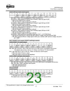
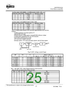
IOCB (ADC control)
PAGE0 (Unused)
7
0
6
0
5
0
4
0
3
0
2
0
1
0
0
0
R/W-1
R/W-1
R/W-1
R/W-1
R/W-1
R/W-1
R/W-1
R/W-1
** This page must clear to 0 or MCU power consumption will increase.
The default value in these 8 bits are “1”. Please clear them to “0” when init MCU.
PAGE1 (ADC control bits)
7
6
5
4
3
2
1
X
-
0
IN2
IN1
IN0
ADCLK1 ADCLK0 ADPWR
ADST
R/W-0
R/W-0
R/W-0
R/W-0
R/W-0 R/W-0 R/W-0
Bit 0(ADST) : AD converter start to sample
By setting to “1”, the AD will start to sample data. This bit will be cleared by hardware automatically after a
sampling.
Bit 1 : (undefined) not allowed to use
Bit 2(ADPWR) : AD converter power control, 1/0 Î enable/disable
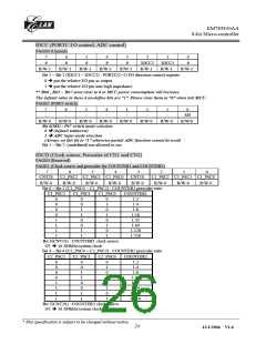
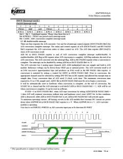
Bit 3 ~ Bit 4 (ADCLK0 ~ ADCLK1) : AD circuit ‘s sampling clock source.
__________________________________________________________________________________________________________________________________________________________________
* This specification is subject to be changed without notice.
22
12/1/2004 V1.6

 ELAN [ ELAN MICROELECTRONICS CORP ]