EM785830AA
8-bit Micro-controller
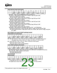
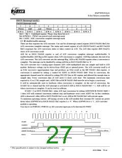
IOCE (Interrupt mask,)
PAGE0 (Interrupt mask)
7
6
5
4
3
2
1
0
PWM2
RBF
ADI
PWM1
0
0
0
0
R/W-0
R/W-0
R/W-0
R/W-0
R/W-0
R/W-0
R/W-0
R/W-0
Bit 0 ~ Bit 3 : Undefined register. Please clear these bits to 0.
Bit 4(PWM1) : PWM1 one period reach interrupt mask.
Bit 5 (ADI) : ADC conversion complete interrupt mask
0/1 Î disable/enable interrupt
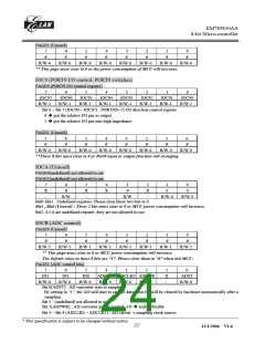
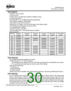
There are four registers for A/D converter. Use one bit of interrupt control register (IOCE PAGE0 Bit5) for
A/D conversion complete interrupt. The status and control register of A/D (IOCB PAGE1 and RE PAGE0
Bit5) responses the A/D conversion status or takes control on A/D. The A/D data register (RB PAGE1)
stores A/D conversion result.
ADI bit in IOCE PAGE0 register is end of A/D conversion complete interrupt enable/disable. It
enables/disables ADI flag in RE register when A/D conversion is complete. ADI flag indicates the end of an
A/D conversion. The A/D converter sets the interrupt flag, ADI in RE PAGE0 register when a conversion is
complete. The interrupt can be disabled by setting ADI bit in IOCE PAGE0 Bit5 to ‘0’.
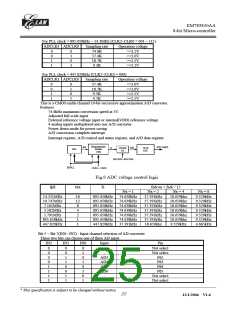
The A/D converter has 4 analog input channels AD3~AD6 multiplexed into one sample and hold to A/D
module. Reference voltage can be driven from VREF pin or internal power. The A/D converter itself is of
an 8-bit successive approximation type and produces an 8-bit result in the RB PAGE1 data register. A
conversion is initiated by setting a control bit ADST in IOCB PAGE1 Bit0. Prior to conversion, the
appropriate channel must be selected by setting IN0~IN1 bits in RE register and allowed for enough time to
sample data. Every conversion data of A/D need 12-clock cycle time. The minimum conversion time
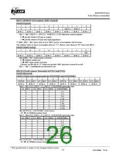
required is 13 us (73K sample rate). ADST Bit in IOCB PAGE1 Bit0 must be set to begin a conversion.
It will be automatically reset in hardware when conversion is complete. At the end of conversion, the
START bit is cleared and the A/D interrupt is activated if ADI in IOCE PAGE0 Bit5 = 1. ADI will be set
when conversion is complete. It can be reset in software.
If ADI = 0 in IOCE PAGE0 Bit5, when A/D start conversion by setting ADST(IOCB PAGE1 Bit0) =
1 then A/D will continue conversion without stop and hardware won’t reset ADST bit. In this condition,
ADI is deactived. After ADI in IOCE PAGE0 bit5 is set, ADI in RE PAGE0 bit5 will activate again.
To minimum operating current , all biasing circuits in the A/D module that consume DC current are power
down when ADPWR bit in IOCB PAGE1 Bit2 register is a ’0’. When ADPWR bit is a ‘1’, A/D converter
module is operating.
User has to set PORT62~PORT65 as AD converter input pin or bi-direction IO PORT
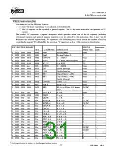
1
2
3
4
5
6
7
8
9
10
START
SAMPLE
ADI(IOCE PAGE0 bit5 ) =1
ADI(RE PAGE0 bit 5)
Clear by software
DATA
Fig.10 A/D converter timing
__________________________________________________________________________________________________________________________________________________________________
* This specification is subject to be changed without notice.
25
12/1/2004 V1.6

 ELAN [ ELAN MICROELECTRONICS CORP ]