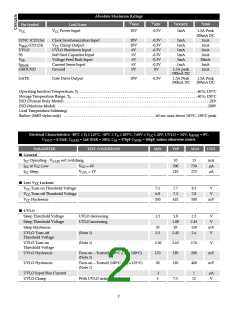
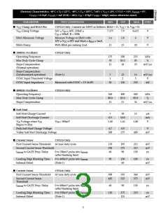
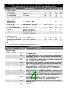
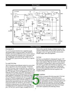
Application Information: continued
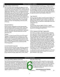
The Line BIAS pin shows a significant change in the regu-
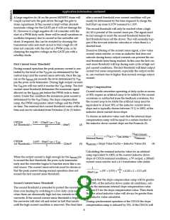
the rising edge of the Gate is shown in Figure 4. When this
pin is held high or low the internal clock determines the
oscillator frequency.
lated VCC voltage when sinking large currents. This will
show up as poor line regulation with a low value pull-up
resistor. Typical regulated VCC vs BIAS pin sink current is
shown in Figure 1.
SYNC
8.3
OSC
GATE
8.2
8.1
Figure 3. Synchronized Operation
8
140
130
120
110
100
90
7.9
5µ
10µA
20µA
50µA
100µA
200µA
Bias Current (I
)
BIAS
Figure 1. Regulated VCC vs BIAS Sink Current
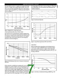
Clock Synchronization Pin (CS5126 Only)
The CS5126 can be synchronized to signals ranging from
30% slower to several times faster than the internal oscilla-
tor frequency. If the part is synchronized to a fast signal,
maximum duty cycle will be reduced as the frequency
increases as shown in Figure 2.
80
70
200kHz
300kHz
400kHz
500kHz
600kHz
Figure 4 : Typical Phase Lag between SYNC and GATE on.
0.82
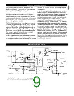
Gate Drive
Rail to rail gate driver operation can be obtained (up to
13.5V) over a range of MOSFET input capacitance if the
gate resistor value is kept low. Figure 5 shows the high
gate drive level vs. the series gate resistance with VCC = 8V
driving an IRF220.
125°C
25°C
0.77
-40°C
0.72
200kHz
8.5
8
300kHz
400kHz
500kHz
600kHz
Frequency
7.5
Figure 2: CS5126 Maximum Duty Cycle vs Frequency (Synchronized
Operation)
7
6.5
If the converter is initially free running and a sync signal is
applied, the current oscillator cycle will terminate and the
oscillator will lock on to the sync signal. The SYNC pin
works with a positive edge triggered signal. When the sync
signal transitions high the current PWM cycle terminates
and a new cycle begins as shown in Figure 3. The typical
phase lag between the rising edge of the SYNC signal and
6
0
0.3
0.5
2.5
5
11
Gate Resistor Value
Figure 5. Gate Drive vs Gate Resistor Driving an IRF220 (VCC = 8V)
7

 CHERRY [ CHERRY SEMICONDUCTOR CORPORATION ]