Electrical Characteristics: -40°C ≤ TJ ≤ 125°C, -40°C ≤ TA ≤ 105°C, 7.60V ≤ VCC ≤ 20V, UVLO = 3.0V, ISENSE = 0V,
V(CC) = 0.33µF, CGATE = 1nF (ESR = 10Ω), CSS = 470pF CV(FB) = 100pF, unless otherwise stated.
C
PARAMETER
TEST CONDITIONS
MIN
TYP
MAX
UNIT
ꢀ Voltage Feedback
VFB Pull-up Res.
2.9
2.63
2.40
460
4.3
2.90
2.65
490
8.1
3.15
2.90
520
kΩ
V
VFB Clamp Voltage
VFB Clamp Voltage
VFB Fault Voltage Threshold
CS5124 Only
CS5126 Only
V
mV
ꢀ Output Gate Drive
Maximum Sleep
VCC = 6.0V, IOUT = 1mA
1.2
2.0
V
Pull-down Voltage
GATE High (AC)
GATE Low (AC)
GATE High Clamp Voltage
Rise Time
Series resistance < 1Ω (Note 1)
Series resistance < 1Ω (Note 1)
VCC = 20V
VCC-1
11.0
VCC-0.5
0.0
V
V
0.5
16.0
65
13.5
45
V
Measure GATE rise time,
ns
1V < GATE < 9V; VCC =12V
Fall Time
Measure GATE fall time,
25
55
ns
9V > GATE > 1V; VCC = 12V
ꢀ Thermal Shutdown
Thermal Shutdown Temperature (Note 1) (GATE low)
135
100
15
150
125
25
165
150
35
°C
°C
°C
Thermal Enable Temperature
Thermal Hysteresis
(Note 1) (GATE switching)
(Note 1)
Notes
1. Not tested in production. Specification is guaranteed by design.
Package Lead Description
FUNCTION
PACKAGE LEAD #
8 Lead SO Narrow
LEAD SYMBOL
CS5124
CS5126
1
2
1
-
VCC
VCC Power Input Pin.
BIAS
VCC Clamp Output Pin. This pin will control the gate of an N-channel MOS-
FET that in turn regulates VCC. This pin is internally clamped at 15V when
the IC is in sleep mode.
-
3
2
SYNC
UVLO
Clock Synchronization Pin. A positive edge will terminate the current PWM
cycle. Ground this pin when it is not used.
3
Sleep and under voltage lockout pin. A voltage greater than 1.8V causes the
chip to "wake up" however the GATE remains low. A voltage greater than
2.6V on this pin allows the output to switch.
4
5
4
5
SS
Soft Start Capacitor Pin. A capacitor placed between SS and GROUND is
charged with 10µA and discharged with 10mA. The Soft Start capacitor con-
trols both soft-start time and hiccup mode frequency.
VFB
Voltage Feedback Pin. The collector of an optocoupler is typically tied to this
pin. This pin is pulled up internally by a 4.3kΩ resistor to 5V and is clamped
internally at 2.9V(2.65V). If VFB is pulled > 4V, the oscillator is disabled and
GATE will stay high. If the VFB pin is pulled < 0.49V, GATE will stay low.
6
6
ISENSE
Current Sense Pin. This pin is connected to the current sense resistor on the
primary side. If VFB is floating, the GATE will go low if ISENSE = 195mV
(335mV). If ISENSE > 275mV (525mV), Soft Start will be initiated.
7
8
7
8
GATE
Gnd
Gate Drive Output Pin. Capable of driving a 3nF load. GATE is nominally
clamped to 13.5V.
Ground Pin.
4

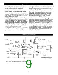
 CHERRY [ CHERRY SEMICONDUCTOR CORPORATION ]