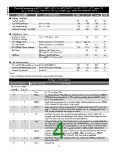
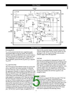
Block Diagram
{CS5126 ONLY}
SYNC
V
CC
V
+
UVLO COMP
CC
F3
DRIVER
OSC
DIS
S
R
Q
R
S
G1
GATE
Q
+
-
V
CC
V
= 5V
REF
F1
RAMP
G2
ENABLE
V
7.7 V/7.275V
RESET DOMAIN
V5
REF
-
{85 mV/us}
170mV us
V5
REF
VREFOK
+
LINE UVLO COMP
-
G7
4500Ω
+
V
G3
-
V5
REF
+
TSHUT
+
V
COMP
FB
+
150°C/125°C
+
V
10µA
2.62 V/2.45V
V
490mV {1/5}
REMOTE
(SLEEP) COMP
1/10
PWM COMP
-
V
÷
FB
+
UVLO
+
+
V
-
{125mV}
60mV
+
V
1000Ω
1.91 V/1.83V
+
BIAS
(CS5124 ONLY)
I
SENSE
{525mV}
275mV
SOFT START LATCH
-
+
2ND I
COMP
F2
V
V
BLANKING
CC
G5
S
R
Q
BLANK
2.9 R
G6
SET DOMAIN
{2.65V}
2.90V
V5REF
LINE AMP
-
-
+
+
SS AMP
+
V
+
R
SS COMP
+
V
2.0V
-
+
V
275mV
1.32V
Gnd
+
SS
V
Theory of Operation
Powering the IC
10µA. As the capacitor charges, a buffered version of the
capacitor voltage appears on the VFB pin and the VFB volt-
age begins to rise. As VFB rises the duty cycle increases
until the supply comes into regulation.
VCC can be powered directly from a regulated supply
and requires 500µA of start-up current. The CS5124/6
includes a line bias pin (BIAS) that can be used to control a
series pass transistor for operation over a wide input volt-
age. The BIAS pin will control the gate voltage of an N-
channel MOSFET placed between VIN and VCC to regulate
VCC at 8V.
Soft Start
Soft Start is accomplished by clamping the VFB pin 1.32V
below the SS pin during normal start up and during restart
after a fault condition. When the CS5124/6 starts, the Soft
Start capacitor is charged from a 10µA source from 0V to
4.9V. The VFB pin follows the Soft Start pin offset by –1.32V
until the supply comes into regulation or until the Soft
Start error amp is clamped at 2.9V (2.65V for the CS5126).
During fault conditions the Soft Start capacitor is dis-
charged at 10mA.
VCC and UVLO Pins
The UVLO pin has three different modes; low power shut-
down, Line UVLO, and normal operation. To illustrate
how the UVLO pin works; assume that VIN, as shown in
the application schematic, is ramped up starting at 0V with
the UVLO pin open. The SS and ISENSE pins also start at 0V.
While the UVLO is below 1.8V, the IC will remain in a low
current sleep mode and the BIAS pin of the CS5124 is inter-
nally clamped to a maximum of 15V. When the voltage on
the UVLO pin rises to between 1.8V and 2.6V the reference
for the VCC UVLO is enabled and VCC is regulated to 8V by
the BIAS pin (CS5124 only), but the IC remains in a UVLO
state and the output driver does not switch. When the
UVLO pin exceeds 2.6V and the VCC pin exceeds 7.7V, the
GATE pin is released from a low state and can begin
switching based on the comparison of the ISENSE and VFB
pins. The Soft Start capacitor begins charging from 0V at
Fault Conditions
The CS5124/6 recognizes the following faults: UVLO off,
Thermal Shutdown, VREF(OK), and Second Current
Threshold. Once a fault is recognized, fault latch F2 is set
and the IC immediately shuts down the output driver and
discharges the Soft Start capacitor. Soft Start will begin
only after all faults have been removed and the Soft Start
capacitor has been discharged to less than 0.275V. Each
fault will be explained in the following sections.
5

 CHERRY [ CHERRY SEMICONDUCTOR CORPORATION ]