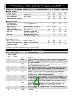
Theory of Operation: continued
for the CS5126) threshold. If the ISENSE voltage exceeds the
Under Voltage Lockout (UVLO)
second threshold, F2 is set, the driver turns off, and the
soft-start capacitor discharges. After the Soft Start capacitor
has discharged to less than 0.275V Soft Start will begin. If
the fault condition has been removed the supply will oper-
ate normally. If the fault remains the supply will operate in
hiccup mode until the fault condition is removed.
The UVLO pin is tied to typically the midpoint of a resis-
tive divider between VIN and GROUND. During a start up
sequence, this pin must be above 2.6V in order for the IC to
begin normal operation. If the IC is running and this pin is
pulled below 1.8V, F2 shuts down the output driver and
discharges the Soft Start capacitor in order to insure proper
start-up. If the UVLO pin is pulled high again before the
Soft Start capacitor discharges, the IC will complete the
Soft Start discharge and, if no other faults are present, will
immediately restart the power supply. If the UVLO pin
stays low, then it will enter either the low current sleep
mode or the UVLO state depending on the level of the
UVLO pin.
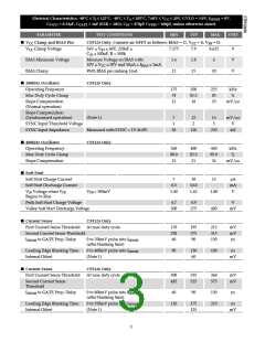
VFB Comparator
The VFB comparator detects when the output voltage is too
high. When the regulated output voltage is too high, the
feedback loop will drive VFB low. If VFB is less than 0.49V
the output of the VFB comparator will go high and shut the
output driver off.
Oscillator
Thermal Shutdown
The internally trimmed, 400kHz (CS5124) or 200kHz
(CS5126) provides the slope compensation ramp as well as
the pulse for enabling the output driver.
If the IC junction temperature exceeds approximately
150°C the thermal shutdown circuit sets F2, which shuts
down the output driver and discharges the Soft Start
capacitor. If no other faults are present the IC will initiate
Soft Start when the IC junction temperature has been
reduced by 25°C.
PWM Comparator and Slope Compensation
The CS5124/6 provides a fixed internal slope compensa-
tion ramp that is subtracted from the feedback signal. The
pwm comparator compares peak primary current to a por-
tion of the difference of the feedback voltage and slope
compensation ramp. The 170mV/µs (85mV/µs for the
CS5126) slope compensation ramp is subtracted from the
voltage feedback signal internally. The difference signal is
then divided by ten (five for the CS5126) before the PWM
comparator to provide high noise rejection with a low volt-
age across the current sense network. (The effective ramp
is 21mV/µs for the CS5124, and 18mV/µs for the CS5126).
A 60mV (125mV for the CS5126) nominal offset on the pos-
itive input to the PWM comparator allows for operation
with the ISENSE pin at, or even slightly below Gnd.
VREF(OK)
VREF(OK) is an internal monitor that insures the internal
regulator is running before any switching occurs. This
function does not trip the fault comparator like the other
fault functions. To insure that Soft Start will occur at low
line conditions the UVLO divider should be set up so that
the VCC UVLO comparator turns on before the LINE
UVLO comparator.
Second Threshold Comparator
Since the maximum dynamic range of the ISENSE signal in
normal operation is 195mV (335mV for the CS5126), any
voltage exceeding this threshold on the ISENSE pin is con-
sidered a fault and the PWM cycle is terminated. The 2nd
ICOMP compares the ISENSE signal with a 275mV (525mV
A 4.3kΩ pull-up resistor internally connected to a 5V nomi-
nal reference provides the bias current to for an opto-cou-
pler connection to the VFB pin.
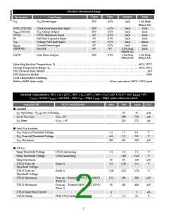
Application Information
UVLO and Thermal Shutdown Interaction
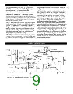
BIAS Pin (CS5124 Only)
The UVLO pin and thermal shutdown circuit share the
The bias pin can be used to control VCC as shown in the
same internal comparator. During high temperature opera- main application diagram. In order to provide adequate
tion (TJ >100°C) the UVLO pin will interact with the ther-
mal shutdown circuit. This interaction increases the turn-
on threshold (and hysteresis) of the UVLO circuit. If the
UVLO pin shuts down the IC during high temperature
operation, higher hysteresis (see hysteresis specification)
might be required to enable the IC.
phase margin for the bias control loop, the pole created by
the series pass transistor and the VCC bypass capacitor
should be kept above 10kHz. The frequency of this pole
can be calculated by Formula (1).
Pole
Transconductance of pass Transistor
Frequency =
(1)
2 × π × CV(CC)
6

 CHERRY [ CHERRY SEMICONDUCTOR CORPORATION ]