VT82C686B
Miscellaneous / General Purpose I/O
Offset 73-70 - Subsystem ID ............................................ WO
................. always reads 0
31-0 Subsystem ID / Vendor ID
Contents may be read at offset 2C.
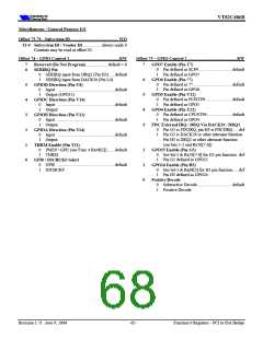
Offset 74 – GPIO Control 1..............................................RW
Offset 75 – GPIO Control 2 ............................................. RW
.................... default = 0
7
6
5
4
3
GPO7 Enable (Pin T7)
7
6
Reserved (Do Not Program)
SERIRQ Pin
0
Pin defined as SLP#............................... default
1
Pin defined as GPO7
0
1
SERIRQ input from DRQ2 (Pin H3)......default
SERIRQ input from DACK5# (Pin L4)
GPO6 Enable (Pin ??)
0
Pin defined as ??.................................... default
5
4
3
2
1
0
GPIOD Direction (Pin U8)
1
Pin defined as GPO6
0
Input .....................................................default
1
Output (GPO11)
GPO5 Enable (Pin V12)
0
Pin defined as PCISTP# ........................ default
GPIOC Direction (Pin V14)
1
Pin defined as GPO5
0
Input .....................................................default
1
Output
GPO4 Enable (Pin Y12)
0
Pin defined as CPUSTP#....................... default
GPIOB Direction (Pin U12)
1
Pin defined as GPO4
0
Input .....................................................default
1
Output
FDC External IRQ / DRQ Via DACK2# / DRQ2
0
1
Pin G5 is FDCIRQ, pin H3 is FDCDRQ .....def
Pin G5 is DACK2# or other alternate function
Pin H3 is DRQ2 or other alternate function
(see bits 1-2 and Rx76[7-6])
GPIOA Direction (Pin T14)
0
Input .....................................................default
1
Output
THRM Enable (Pin T11)
0
PME# / GPI5 (see Func 4 Rx48[5]).......default
2
1
0
GPO25 Enable (Pin G5)
0
See bit-3 & Rx76[7-6] for G5 pin function..def
1
THRM
1
Pin G5 defined as GPO25
GPI0 / IOCHCK# Select
0
GPI0 .....................................................default
GPO24 Enable (Pin H3)
0
See bit-3 & Rx68[3] for H3 pin function.....def
1
IOCHCK#
1
Pin H3 defined as GPO24
Positive Decode
0
Subtractive Decode................................ default
1
Positive Decode
Revision 1.71 June 9, 2000
-62-
Function 0 Registers - PCI to ISA Bridge

 ETC [ ETC ]