VT82C686B
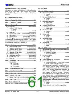
Offset 42 - ISA Clock Control. .........................................RW
Offset 43 - ROM Decode Control.................................... RW
Setting these bits enables the indicated address range to be
included in the ROMCS# decode:
7
6
5
Latch IO16#
0
Enable (recommended setting)...............default
1
Disable
..........................default=0
...........................default=0
............................default=0
.............................default=0
.............................default=0
.............................default=0
.............................default=0
.............................default=0
7
6
5
4
3
2
1
0
FFFE0000h-FFFEFFFFh
FFF80000h-FFFDFFFFh
FFF00000h-FFF7FFFFh
000E0000h-000EFFFFh
000D8000h-000DFFFFh
000D0000h-000D7FFFh
000C8000h-000CFFFFh
000C0000h-000C7FFFh
MCS16# Output
0
Disable ...................................................default
1
Enable
(do not program)
Master Request Test Mode
0
1
Disable ...................................................default
Enable
................... default = 0
4
3
Reserved (Do Not Program)
ISA Clock (BCLK) Select Enable
0
1
BCLK = PCICLK / 4..............................default
BCLK selected per bits 2-0
Offset 44 - Keyboard Controller Control ....................... RW
(do not program)........default = 0
KBC Timeout Test
7
(if bit-3 = 1)
2-0 ISA Bus Clock Select
(do not program)........................default = 0
6-4 Reserved
000 BCLK = PCICLK / 3..............................default
001 BCLK = PCICLK / 2
010 BCLK = PCICLK / 4
011 BCLK = PCICLK / 6
100 BCLK = PCICLK / 5
101 BCLK = PCICLK / 10
110 BCLK = PCICLK / 12
111 BCLK = OSC / 2
3
Mouse Lock Enable
0
Disable................................................... default
1
Enable
(do not program)........................default = 0
(no function) ..............................default = 0
2-1 Reserved
Reserved
0
Offset 45 - Type F DMA Control .................................... RW
7
ISA Master / DMA to PCI Line Buffer
0
1
Disable................................................... default
Enable
Note: Procedure for ISA Clock switching:
1) Set bit 3 to 0; 2) Change value of bit 2-0; 3) Set bit 3 to 1
............default=0
............default=0
............default=0
............default=0
............default=0
............default=0
............default=0
6
5
4
3
2
1
0
DMA type F Timing on Channel 7
DMA type F Timing on Channel 6
DMA type F Timing on Channel 5
DMA type F Timing on Channel 3
DMA type F Timing on Channel 2
DMA type F Timing on Channel 1
DMA type F Timing on Channel 0
Note: For bits 0-6 above, see also Rx41[3]
Revision 1.71 June 9, 2000
-56-
Function 0 Registers - PCI to ISA Bridge

 ETC [ ETC ]