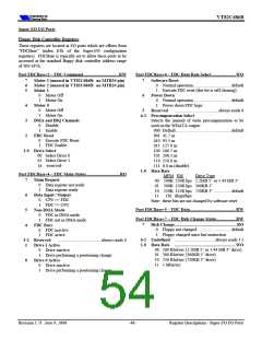
VT82C686B
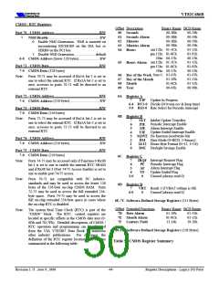
CMOS / RTC Registers
Offset Description
00 Seconds
01 Seconds Alarm
02 Minutes
03 Minutes Alarm
04 Hours
Binary Range BCD Range
00-3Bh
00-3Bh
00-59h
00-59h
00-59h
00-59h
01-12h
81-92h
00-23h
01-12h
81-92h
00-23h
01-07h
01-31h
01-12h
00-99h
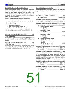
Port 70 - CMOS Address..................................................RW
......................................................... RW
NMI Disable
7
00-3Bh
00-3Bh
0
Enable NMI Generation. NMI is asserted on
encountering IOCHCK# on the ISA bus or
SERR# on the PCI bus.
am 12hr: 01-1Ch
pm 12hr: 81-8Ch
24hr: 00-17h
am 12hr: 01-1Ch
pm 12hr: 81-8Ch
24hr: 00-17h
Sun=1: 01-07h
1
Disable NMI Generation ........................default
(lower 128 bytes)....................... RW
6-0 CMOS Address
Port 71 - CMOS Data........................................................RW
(128 bytes)
05 Hours Alarm
7-0 CMOS Data
06 Day of the Week
07 Day of the Month
08 Month
Note: Ports 70-71 may be accessed if Rx5A bit-2 is set to
one to select the internal RTC. If Rx5A bit-2 is set to
zero, accesses to ports 70-71 will be directed to an
external RTC.
01-1Fh
01-0Ch
00-63h
09 Year
Port 72 - CMOS Address..................................................RW
0A Register A
Update In Progress
Divide (010=ena osc & keep time)
Rate Select for Periodic Interrupt
7
UIP
(256 bytes)................................. RW
7-0 CMOS Address
Port 73 - CMOS Data........................................................RW
(256 bytes)
6-4 DV2-0
3-0 RS3-0
7-0 CMOS Data
0B Register B
SET
Note: Ports 72-73 may be accessed if Rx5A bit-2 is set to
one to select the internal RTC. If Rx5A bit-2 is set to
zero, accesses to ports 72-73 will be directed to an
external RTC.
Inhibit Update Transfers
Periodic Interrupt Enable
Alarm Interrupt Enable
Update Ended Interrupt Enable
No function (read/write bit)
Data Mode (0=BCD, 1=binary)
Hours Byte Format (0=12, 1=24)
Daylight Savings Enable
7
6
5
4
3
2
1
0
PIE
AIE
UIE
SQWE
DM
24/12
DSE
Port 74 - CMOS Address..................................................RW
(256 bytes)................................. RW
7-0 CMOS Address
Port 75 - CMOS Data........................................................RW
(256 bytes)
7-0 CMOS Data
0C Register C
Interrupt Request Flag
Periodic Interrupt Flag
Alarm Interrupt Flag
Update Ended Flag
7
6
5
4
3-0
IRQF
Note: Ports 74-75 may be accessed only if Function 0 Rx5B
bit-1 is set to one to enable the internal RTC SRAM
and if Rx48 bit-3 (Port 74/75 Access Enable) is set to
one to enable port 74/75 access.
PF
AF
UF
0
Unused (always read 0)
Note: Ports 70-71 are compatible with PC industry-
standards and may be used to access the lower 128
bytes of the 256-byte on-chip CMOS RAM. Ports
72-73 may be used to access the full extended 256-
byte space. Ports 74-75 may be used to access the
full on-chip extended 256-byte space in cases where
the on-chip RTC is disabled.
0D Register D
Reads 1 if VBAT voltage is OK
Unused (always read 0)
7
VRT
6-0
0
(111 Bytes)
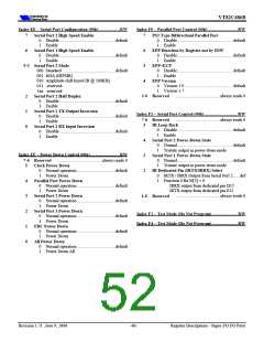
0E-7C Software-Defined Storage Registers
Offset Extended Functions
7D Date Alarm
7E Month Alarm
7F Century Field
Binary Range BCD Range
Note: The system Real Time Clock (RTC) is part of the
“CMOS” block. The RTC control registers are
located at specific offsets in the CMOS data area (0-
0Dh and 7D-7Fh). Detailed descriptions of CMOS /
RTC operation and programming can be obtained
from the VIA VT82887 Data Book or numerous
01-1Fh
01-0Ch
13-14h
01-31h
01-12h
19-20h
(128 Bytes)
80-FF Software-Defined Storage Registers
Table 5. CMOS Register Summary
other industry publications.
For reference, the
definition of the RTC register locations and bits are
summarized in the following table:
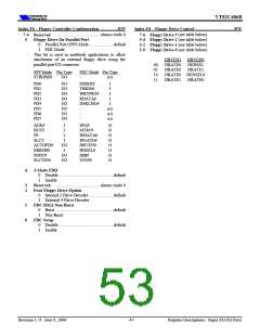
Revision 1.71 June 9, 2000
-44-
Register Descriptions - Legacy I/O Ports

 ETC [ ETC ]