VT82C686B
DMA Controller I/O Registers
Ports 00-0F - Master DMA Controller
Ports 80-8F - DMA Page Registers
Channels 0-3 of the Master DMA Controller control System
DMA Channels 0-3. There are 16 Master DMA Controller
registers:
There are eight DMA Page Registers, one for each DMA
channel. These registers provide bits 16-23 of the 24-bit
address for each DMA channel (bits 0-15 are stored in
registers in the Master and Slave DMA Controllers). They are
located at the following I/O Port addresses:
I/O Address Bits 15-0 Register Name
0000 0000 000x 0000
0000 0000 000x 0001
0000 0000 000x 0010
0000 0000 000x 0011
0000 0000 000x 0100
0000 0000 000x 0101
0000 0000 000x 0110
0000 0000 000x 0111
0000 0000 000x 1000
0000 0000 000x 1001
0000 0000 000x 1010
0000 0000 000x 1011
0000 0000 000x 1100
0000 0000 000x 1101
0000 0000 000x 1110
0000 0000 000x 1111
Ch 0 Base / Current Address
Ch 0 Base / Current Count
Ch 1 Base / Current Address
Ch 1 Base / Current Count
Ch 2 Base / Current Address
Ch 2 Base / Current Count
Ch 3 Base / Current Address
Ch 3 Base / Current Count
Status / Command
Write Request
Write Single Mask
Write Mode
Clear Byte Pointer F/F
Master Clear
RW
RW
RW
RW
RW
RW
RW
RW
RW
WO
WO
WO
WO
WO
WO
RW
I/O Address Bits 15-0 Register Name
0000 0000 1000 0111
0000 0000 1000 0011
0000 0000 1000 0001
0000 0000 1000 0010
Channel 0 DMA Page (M-0).........RW
Channel 1 DMA Page (M-1).........RW
Channel 2 DMA Page (M-2).........RW
Channel 3 DMA Page (M-3).........RW
0000 0000 1000 1111
0000 0000 1000 1011
0000 0000 1000 1001
0000 0000 1000 1010
Channel 4 DMA Page (S-0) ..........RW
Channel 5 DMA Page (S-1) ..........RW
Channel 6 DMA Page (S-2) ..........RW
Channel 7 DMA Page (S-3) .........RW
DMA Controller Shadow Registers
The DMA Controller shadow registers are enabled by setting
function 0 Rx77 bit 0. If the shadow registers are enabled,
they are read back at the indicated I/O port instead of the
standard DMA controller registers (writes are unchanged).
Clear Mask
R/W All Mask Bits
Ports C0-DF - Slave DMA Controller
Port 0 –Channel 0 Base Address ...................................... RO
Port 1 –Channel 0 Byte Count.......................................... RO
Port 2 –Channel 1 Base Address ...................................... RO
Port 3 –Channel 1 Byte Count.......................................... RO
Port 4 –Channel 2 Base Address ...................................... RO
Port 5 –Channel 2 Byte Count.......................................... RO
Port 6 –Channel 3 Base Address ...................................... RO
Port 7 –Channel 3 Byte Count.......................................... RO
Port 8 –1st Read Channel 0-3 Command Register .......... RO
Port 8 –2nd Read Channel 0-3 Request Register.............. RO
Port 8 –3rd Read Channel 0 Mode Register..................... RO
Port 8 –4th Read Channel 1 Mode Register ..................... RO
Port 8 –5th Read Channel 2 Mode Register ..................... RO
Port 8 –6th Read Channel 3 Mode Register ..................... RO
Channels 0-3 of the Slave DMA Controller control System
DMA Channels 4-7. There are 16 Slave DMA Controller
registers:
I/O Address Bits 15-0 Register Name
0000 0000 1100 000x
0000 0000 1100 001x
0000 0000 1100 010x
0000 0000 1100 011x
0000 0000 1100 100x
0000 0000 1100 101x
0000 0000 1100 110x
0000 0000 1100 111x
0000 0000 1101 000x
0000 0000 1101 001x
0000 0000 1101 010x
0000 0000 1101 011x
0000 0000 1101 100x
0000 0000 1101 101x
0000 0000 1101 110x
0000 0000 1101 111x
Ch 4 Base / Current Address
Ch 4 Base / Current Count
Ch 5 Base / Current Address
Ch 5 Base / Current Count
Ch 6 Base / Current Address
Ch 6 Base / Current Count
Ch 7 Base / Current Address
Ch 7 Base / Current Count
Status / Command
Write Request
Write Single Mask
Write Mode
Clear Byte Pointer F/F
Master Clear
RW
RW
RW
RW
RW
RW
RW
RW
RW
WO
WO
WO
WO
WO
WO
WO
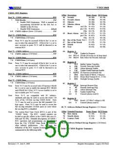
Port F –Channel 0-3 Read All Mask................................ RO
Port C4 –Channel 5 Base Address.................................... RO
Port C6 –Channel 5 Byte Count....................................... RO
Port C8 –Channel 6 Base Address.................................... RO
Port CA –Channel 6 Byte Count...................................... RO
Port CC –Channel 7 Base Address................................... RO
Port CE –Channel 7 Byte Count ...................................... RO
Clear Mask
Read/Write All Mask Bits
Note that not all bits of the address are decoded.
Port D0 –1st Read Channel 4-7 Command Register........ RO
Port D0 –2nd Read Channel 4-7 Request Register........... RO
Port D0 –3rd Read Channel 4 Mode Register.................. RO
Port D0 –4th Read Channel 5 Mode Register .................. RO
Port D0 –5th Read Channel 6 Mode Register .................. RO
Port D0 –6th Read Channel 7 Mode Register .................. RO
The Master and Slave DMA Controllers are compatible with
the Intel 8237 DMA Controller chip. Detailed description of
8237 DMA controller operation can be obtained from the Intel
Peripheral Components Data Book and numerous other
industry publications.
Port DE –Channel 4-7 Read All Mask............................. RO
Revision 1.71 June 9, 2000
-42-
Register Descriptions - Legacy I/O Ports

 ETC [ ETC ]