VS1005g Datasheet
7
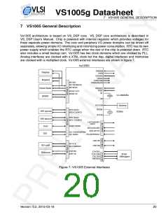
VS1005 GENERAL DESCRIPTION
buttons.
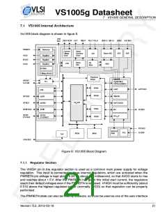
A power-on reset monitors the core voltage and asserts reset if CVDD drops below the CMON
level. It is also possible to force a reset by keeping PWRBTN pressed for longer than approx-
imately 5.6 seconds. This feature can be disabled by software. A watchdog counter and the
XRESET pin can also generate a reset for the device.
Resets do not cause the regulators to shut down, but they restore the default regulator voltages.
After boot the firmware and user software can change the voltages.
Return to power-off is possible only with active software control (VSDSP writes the regulator
shutdown bits), or when VHIGH voltage is removed for a sufficiently long time. In the default
firmware player the power button has to be pressed for 2 seconds to make the software power-
down the system and turn the regulators off.
7.1.2 IO Section
IOVDD is used for the level-shifters of the digital I/O and crystal oscillator. The regulated IO
voltage is internally connected. The IOVDD regulator output must be connected to IOVDD1,
IOVDD2 and IOVDD3 input pins. Proper bypass capacitors should also be used.
The firmware uses GPIO0_7 to select I/O voltage level. After reset the I/O voltage is 1.8 V. If
GPIO0_7 has a pull-down resistor, 1.8 V I/O voltage is used. If GPIO0_7 has a pull-up resistor,
3.3 V I/O voltage is used.
7.1.3 Digital Section
All digital logic except the real time clock is powered from core voltage CVDD. The regulated
core voltage is internally connected. The CVDD regulator output must be connected to CVDD1,
CVDD2 and CVDD3 input pins. CVDD pins should have proper bypass capacitors.
Real time clock power pin can be connected to CVDD net or it can have its own power supply
which enables its use during chip power-down. The inputs and outputs of the RTC logic have
level shifters but the RTCVDD voltage should not exceed the CVDD voltage range.
Clock
The crystal amplifier uses a crystal connected to XTALI and XTALO. An external logic-level input
clock can also be used. When VS1005 is used with FS USB, 12 MHz crystal allows lower power
consumption. With FS/HS USB the input clock of 12 MHz or 12.288 MHz is recommended.
An internal phase-locked loop (PLL) generates the internal clock by multiplying the input clock
by 1.0×, 1.5×, . . . , 8.0×. When USB is connected, the clock is 5.0×12 MHz = 60 MHz. When
the player is active, the clock will be automatically changed according to the requirements of
the song being played.
XRESET disables the clock buffer and puts the digital section into powerdown mode.
Version: 0.2, 2012-03-16
22

 ETC [ ETC ]