VS1005g Datasheet
5
PACKAGE AND PIN DESCRIPTIONS
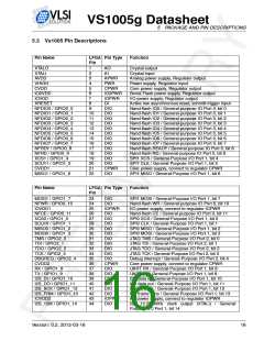
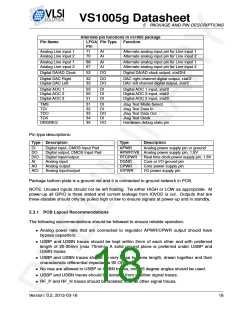
Alternate pin functions in vs1005 package
Pin Name
LFGA Pin Type
Function
Pin
Analog Line input 1
Analog Line input 2
71
70
AI
AI
Alternate analog input pin for Line input 1
Alternate analog input pin for Line input 2
Analog Line input 1
Analog Line input 2
68
67
AI
AI
Alternate analog input pin for Line input 1
Alternate analog input pin for Line input 2
Digital DA/AD Clock
52
DO
Digital DA/AD clock output, xtal/2/4
Digital DAC Right
Digital DAC Left
32
33
DO
DO
DAC right channel digital output, xtal/2
DAC left channel digital output, xtal/2
Digital ADC 1
Digital ADC 2
Digital ADC 3
53
55
51
DI
DI
DI
Digital ADC 1 input, xtal/2
Digital ADC 2 input, xtal/2
Digital ADC 3 input, xtal/2
TMS
TDI
TDO
TCK
31
32
33
34
35
DI
DI
DO
DI
DO
Jtag Test Mode Select
Jtag Test Data In
Jtag Test Data Out
Jtag Test Clock
DBGREQ
Hardware debug state pin
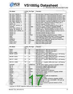
Pin type descriptions:
Type Description
Type
APWR
Description
Analog power supply pin or ground
DI
Digital input, CMOS Input Pad
DO
DIO
AI
Digital output, CMOS Input Pad
Digital input/output
Analog input
APWR1V8 Analog power supply pin, 1.8V
RTCPWR
DGND
Real time clock power supply pin, 1.8V
Core or I/O ground pin
AO
AIO
Analog output
Analog input/output
CPWR
IOPWR
Core power supply pin
I/O power supply pin
Package bottom plate is a ground net and it is connected to ground network in PCB.
NOTE: Unused inputs should not be left floating. Tie either HIGH or LOW as appropriate. At
power-up all GPIO is three stated and current leakage from IOVDD is cut. Outputs that are
three-statable should only be pulled high or low to ensure signals at power-up and in standby.
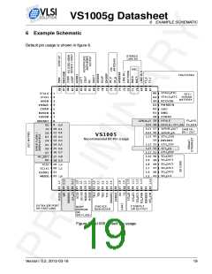
5.3.1 PCB Layout Recommendations
The following recommendations should be followed to ensure reliable operation.
• Analog power nets that are connected to regulator APWR/CPWR output should have
bypass capasitors.
• USBP and USBN traces should be kept within 2mm of each other and with preferred
length of 20-30mm (max 75mm). A solid ground plane is preferred under USBP and
USBN traces.
• USBP and USBN traces should be very close to same length, drawn together and their
characteristic differential impedance 90 Ohms
• No vias are allowed in USBP or USBN traces, only 45 degree angles should be used.
• USBP and USBN traces should be isolated from all other signal traces.
• RF_P and RF_N traces should be isolated from all other signal traces.
Version: 0.2, 2012-03-16
18

 ETC [ ETC ]