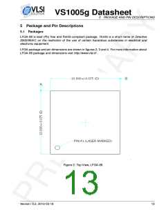
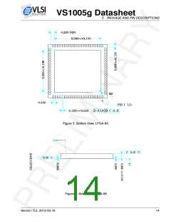
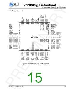
VS1005g Datasheet
5
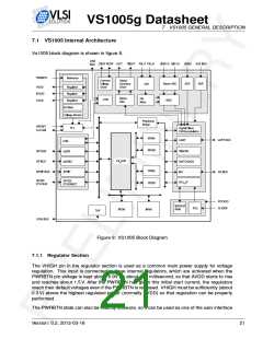
PACKAGE AND PIN DESCRIPTIONS
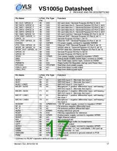
Pin Name
LFGA Pin Type
Pin
Function
SD_CLK / GPIO2_5
SD_DAT0 / GPIO2_6
SD_DAT1 / GPIO2_7
SD_DAT2 / GPIO2_8
SD_DAT3 / GPIO2_9
SD_CMD / GPIO2_10
ETH_RXP / GPIO2_11
GPIO1_15
ETH_TXP / GPIO2_12
IOVDD3
ETH_TXN / GPIO2_13
SPDIF_IN / GPIO0_12
45
46
47
48
49
50
51
52
53
54
55
56
DIO
DIO
DIO
DIO
DIO
DIO
DIO
DIO
DIO
IOPWR
DIO
DIO
DIO
DIO
DIO
CPWR
DI
SD card clock / General-Purpose I/O Port 2, bit 5
SD card data line 0 / General-Purpose I/O Port 2, bit 6
SD card data line 1 / General-Purpose I/O Port 2, bit 7
SD card data line 2 / General-Purpose I/O Port 2, bit 8
SD card data line 3 / General-Purpose I/O Port 2, bit 9
SD card cmd line / General-Purpose I/O Port 2, bit 10
Ethernet RXP / General-Purpose I/O Port 2, bit 11
General-Purpose I/O Port 1, bit 15
Ethernet TXP / General-Purpose I/O Port 2, bit 12
I/O power supply, connect to regulator IOPWR
Ethernet TXN / General-Purpose I/O Port 2, bit 13
S/PDIF data in / General-Purpose I/O Port 0, bit 12
S/PDIF data out / General-Purpose I/O Port 0, bit 13
General-Purpose I/O Port 0, bit 14
SPDIF_OUT / GPIO0_13 57
GPIO0_14
GPIO0_15
VDD3
DBG
TEST
PWRBTN
RTCVDD
XTALO_RTC
XTALI_RTC
58
59
60
61
62
63
64
65
66
General-Purpose I/O Port 0, bit 15
Core power supply, connect to regulator CPWR
Debug mode enable (active high), connect to DGND
Test mode input (active high), connect to DGND
Power button for Regulator startup (and Power Key)
DI
AIO
RTCPWR Real time clock power supply
AO
AI
Real time clock crystal output
Real time clock crystal input
Pin Name
LFGA Pin Type
Pin
Function
AUX0
AUX1
AUX2 / LINE3
MIC2P / AUX3
67
68
69
70
AI
AI
AI
AI
SAR A/D input 0 / Alternate line input 2
SAR A/D input 1 / Alternate line input 1
SAR A/D input 2 / Line input 3
Microphone 2 positive differential input, self-biasing /
SAR A/D input 3 / Alternate line input 2
Microphone 2 negative differential input, self-biasing /
SAR A/D input 4 / Alternate line input 1
Microphone 1 positive differential input, self-biasing /
line input 1
MIC2N / AUX4
MIC1P / LINE1
MIC1N / LINE2
71
72
73
AI
AI
AI
Microphone 1 negative differential input, self-biasing /
line input 2
AVDDRF
RF_N
74
75
76
77
78
79
80
81
82
83
84
85
86
87
88
APWR1V8 1.8V RF power supply, connect to regulator CPWR
AI
AI
APWR
AIO
APWR
AO
FM antenna negative differential input
FM antenna positive differential input
Analog reference ground
Filtering capacitance for reference
Analog power supply, connect to regulator APWR
Right channel output
RF_P
AGND
1
RCAP
AVDD0
RIGHT
N/A
CBUF
LEFT
AVDD1
USBP
USBN
GNDUSB
PWM
N/A
Not connected pin
AO
AO
Common voltage buffer for headphones
Left channel output
APWR
AIO
AIO
APWR
DO
Analog power supply, connect to regulator APWR
USB differential + in / out, controllable 1.5kΩ pull-up
USB differential - in / out
USB ground, connect to ground network in PCB
PWM output
1
Connect to RCAP capasitor without vias in pcb board.
Version: 0.2, 2012-03-16
17

 ETC [ ETC ]