VS1005g Datasheet
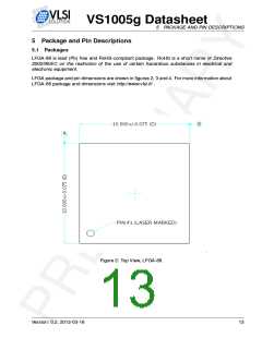
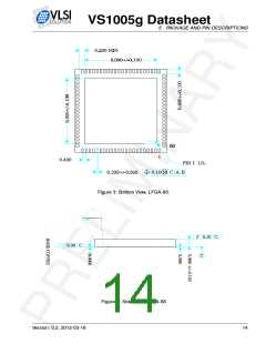
5
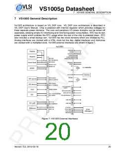
PACKAGE AND PIN DESCRIPTIONS
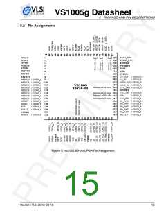
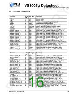
5.3 Vs1005 Pin Descriptions
Pin Name
LFGA Pin Type
Pin
Function
XTALO
XTALI
1
2
AO
AI
Crystal output
Crystal input
AVDD
VHIGH
CVDD
IO2VDD
IOVDD
XRESET
NFDIO0 / GPIO0_0
NFDIO1 / GPIO0_1
NFDIO2 / GPIO0_2
NFDIO3 / GPIO0_3
NFDIO4 / GPIO0_4
NFDIO5 / GPIO0_5
NFDIO6 / GPIO0_6
NFDIO7 / GPIO0_7
NFRDY / GPIO0_8
NFRD / GPIO0_9
XCS1 / GPIO1_4
SCLK1 / GPIO1_5
CVDD1
3
4
5
6
7
8
9
10
11
12
13
14
15
16
17
18
19
20
21
22
APWR
PWR
CPWR
IO2PWR
IOPWR
DI
DIO
DIO
DIO
DIO
DIO
DIO
DIO
DIO
DIO
DIO
DIO
DIO
Analog power supply, Regulator output
Power supply, Regulator input
Core power supply, Regulator output
Serial Flash power supply, Regulator output
I/O power supply, Regulator output
Active low asynchronous reset, schmitt-trigger input
Nand-flash IO0 / General-purpose IO Port 0, bit 0
Nand-flash IO1 / General-purpose IO Port 0, bit 1
Nand-flash IO2 / General-purpose IO Port 0, bit 2
Nand-flash IO3 / General-purpose IO Port 0, bit 3
Nand-flash IO4 / General-purpose IO Port 0, bit 4
Nand-flash IO5 / General-purpose IO Port 0, bit 5
Nand-flash IO6 / General-purpose IO Port 0, bit 6
Nand-flash IO7 / General-purpose IO Port 0, bit 7
Nand-flash READY / General-purpose IO Port 0, bit 8
Nand-flash RD / General-purpose IO Port 0, bit 9
SPI1 XCS / General-Purpose I/O Port 1, bit 4
SPI1 CLK / General-Purpose I/O Port 1, bit 5
Core power supply, connect to regulator CPWR
SPI1 MISO / General-Purpose I/O Port 1, bit 6
CPWR
DIO
MISO1 / GPIO1_6
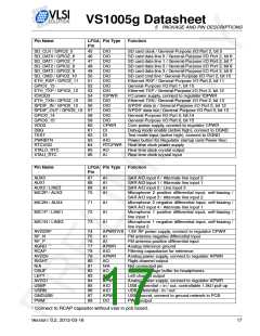
Pin Name
LFGA Pin Type
Pin
Function
MOSI1 / GPIO1_7
NFWR / GPIO0_10
IOVDD1
NFCE / GPIO0_11
XCS0 / GPIO1_0
SCLK0 / GPIO1_1
MISO0 / GPIO1_2
MOSI0 / GPIO1_3
TMS / GPIO2_0
TDI / GPIO2_1
TDO / GPIO2_2
TCK / GPIO2_3
DBGREQ / GPIO2_4
CVDD2
RX / GPIO1_8
TX / GPIO1_9
23
24
25
26
27
28
29
30
31
32
33
34
35
36
37
38
39
40
41
42
43
44
DIO
DIO
IOPWR
DIO
DIO
DIO
DIO
DIO
DIO
DIO
DIO
DIO
DIO
CPWR
DIO
DIO
DIO
DIO
SPI1 MOSI / General-Purpose I/O Port 1, bit 7
Nand-flash WR / General-purpose IO Port 0, bit 10
I/O power supply, connect to regulator IOPWR
Nand-flash CE / General-purpose IO Port 0, bit 11
SPI0 XCS / General-Purpose I/O Port 1, bit 0
SPI0 CLK / General-Purpose I/O Port 1, bit 1
SPI0 MISO / General-Purpose I/O Port 1, bit 2
SPI0 MOSI / General-Purpose I/O Port 1, bit 3
JTAG TMS / General-Purpose I/O Port 2, bit 0
JTAG TDI / General-Purpose I/O Port 2, bit 1
JTAG TDO / General-Purpose I/O Port 2, bit 2
JTAG TCK / General-Purpose I/O Port 2, bit 3
Debug interrupt / General-Purpose I/O Port 2, bit 4
Core power supply, connect to regulator CPWR
UART RX / General-Purpose I/O Port 1, bit 8
UART TX / General-Purpose I/O Port 1, bit 9
I2S data in / General-Purpose I/O Port 1, bit 10
I2S data out / General-Purpose I/O Port 1, bit 11
I2S bit clock / General-Purpose I/O Port 1, bit 12
I2S frame sync / General-Purpose I/O Port 1, bit 13
I/O power supply, connect to regulator IOPWR
I2S 12.288 MHz clock output (XTALI) / General-
Purpose I/O Port 1, bit 14
I2S_DI / GPIO1_10
I2S_DO / GPIO1_11
I2S_BCK / GPIO1_12
I2S_FRM / GPIO1_13
IOVDD2
DIO
DIO
IOPWR
DIO
I2S_12M / GPIO1_14
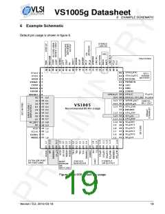
Version: 0.2, 2012-03-16
16

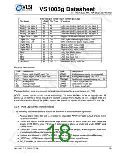
 ETC [ ETC ]