Application Hints (Continued)
e
e
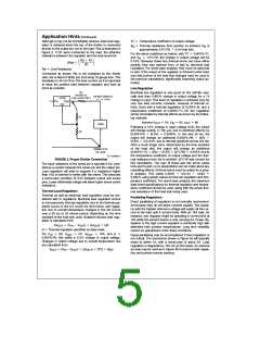
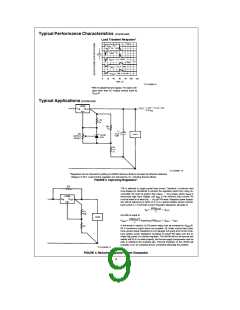
Although it may not be immediately obvious, best load regu-
lation is obtained when the top of the divider is connected
directly to the output pin, not to the load. This is illustrated in
Figure 2. If R1 were connected to the load, the effective
resistance between the regulator and the load would be
TC
Temperature coefficient of output voltage.
Thermal resistance from junction to ambient. i is
i
jA
jA
a
approximately 0.5 C/W
i of heat sink.
§
For the same conditions as before, with TC
and i
0.18%. Because these two thermal terms can have either
polarity, they may subtract from, or add to, electrical load
regulation. For worst-case analysis, they must be assumed
to add. If the output of the regulator is trimmed under load,
only that portion of the load that changes need be used in
the previous calculations, significantly improving output ac-
curacy.
e
1.5 C/W, the change in output voltage will be
0.003%/ C,
§
e
§
jA
a
R2
R1
c
(Rw)
R1
#
J
e
Rw
Line Resistance
Connected as shown, Rw is not multiplied by the divider
ratio. Rw is about 0.004X per foot using 16 gauge wire. This
translates to 40 mV/ft at 10A load current, so it is important
to keep the positive lead between regulator and load as
short as possible.
Line Regulation
Electrical line regulation is very good on the LM196Ðtypi-
cally less than 0.005% change in output voltage for a 1V
change in input. This level of regulation is achieved only for
very low load currents, however, because of thermal ef-
fects. Even with a thermal regulation of 0.002%.W, and a
temperature coefficient of 0.003%/ C, DC line regulation
§
will be dominated by thermal effects as shown by the follow-
ing example:
e
e
e
9V, I
OUT
Assume V
5V, V
8A
OUT
IN
Following a 10% change in input voltage (0.9), the output
s
will change quickly ( 100 ms), due to electrical effects, by
c
e
(0.005%V)
(0.9V)
0.0045%. In the next 20 ms, the
c
c
output will change an additional (0.002%/W) (8A)
e
0.0144% due to thermal gradients across the die.
(0.9V)
After a much longer time, determined by the time constant
of the heat sink, the output will change an additional
c
c
c
the temperature coefficient of output voltage and the ther-
e
(2 C/W) 0.043% due to
(0.003%/ C)
(8A)
(0.9V)
§
§
TL/H/9059–2
mal resistance from die to ambient. (2 C/W was chosen for
FIGURE 2. Proper Divider Connection
§
this calculation). The sign of these last two terms varies
from part to part, so no assumptions can be made about any
cancelling effects. All three terms must be added for a prop-
The input resistance of the sense pin is typically 6 kX, mod-
eled as a resistor between the sense pin and the output pin.
Load regulation will start to degrade if a resistance higher
than 10X is inserted in series with the sense. This assumes
a worst-case condition of 0.5V between output and sense
pins. Lower differential voltage will allow higher sense series
resistance.
a
a
e
0.043
er analysis. This yields 0.0045
0.0144
0.062% using typical values for thermal regulation and tem-
perature coefficient. For worst-case analysis, the maximum
data sheet specifications for thermal regulation and temper-
ature coefficient should be used, along with the actual ther-
mal resistance of the heat sink being used.
Thermal Load Regulation
Thermal, as well as electrical, load regulation must be con-
sidered with IC regulators. Electrical load regulation occurs
in microseconds, thermal regulation due to die thermal gra-
dients occurs in the 0.2 ms-20 ms time frame, and regula-
tion due to overall temperature changes in the die occurs
over a 20 ms to 20 minute period, depending on the time
constant of the heat sink used. Gradient induced load regu-
lation is calculated from
Paralleling Regulators
Direct paralleling of regulators is not normally recommend-
ed because they do not share currents equally. The regula-
tor with the highest reference voltage will supply all the cur-
rent to the load until it current limits. With an 18A load, for
instance, one regulator might be operating in current limit at
16A while the second device is only carrying 2A. Power dis-
sipation in the high current regulator is extremely high with
attendant high junction temperatures. Long term reliability
cannot be guaranteed under these conditions.
e
b
c
c
)
OUT
DV
(V
V
OUT
)
(DI
(b)
OUT
IN
e
b
Thermal regulation specified on data sheet.
e
e
e
OUT
e
10A, and b
For V
9V, V
OUT
5V, DI
IN
Quasi-paralleling may be accomplished if load regulation is
not critical. The connection shown in Figure 5a will typically
share to within 1A, with a worst-case of about 3A. Load
regulation is degraded by 150 mV at 20A loads. An external
op amp may be used as inFigure 5b to improve load regula-
tion and provide remote sensing.
0.005%/W, this yields a 0.2% change in output voltage.
Changes in output voltage due to overall temperature rise
are calculated from
e
b
c
c c
(TC) (i )
jA
V
(V
V
)
(DI
)
OUT
IN
OUT
OUT
5

 ETC [ ETC ]