Application Hints (Continued)
The actual heat sink chosen for the LM196 will be deter-
mined by the worst-case continuous full load current, input
voltage and maximum ambient temperature. Overload or
short circuit output conditions do not normally have to be
considered when selecting a heat sink because the thermal
shutdown built into the LM196 will protect it under these
conditions. An exception to this is in situations where the
regulator must recover very quickly from overload. The
LM196 may take some time to recover to within specified
output tolerance following an extended overload, if the regu-
lator is cooling from thermal shutdown temperature (approx-
imately 175 ) to specified operating temperature (125 C or
quent cost savings in the transformer and heat sink. Some-
times several capacitors in parallel are better to decrease
series resistance and increase heat dissipating area.
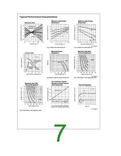
After the raw supply characteristics have been determined,
and worst-case power dissipation in the LM196 is known,
the heat sink thermal resistance can be found from the
graphs titled Maximum Heat Sink Thermal Resistance.
These curves indicate the minimim size heat sink required
as a function of ambient temperature. They are derived from
a case-to-control area thermal resistance of 0.5 C/W and a
§
case-to-power transistor thermal resistance of 1.2 C/W.
§
0.2 C/W is assumed for interface resistance. A maximum
§
§
§
control area temperature of 150 C is used for the LM196
150 C). The procedure for heat sink selection is as follows:
§
Calculate worst-case continuous average power dissipa-
§
and 125 C for the LM396. Maximum power transistor tem-
§
perature is 200 C for the LM196 and 175 C for the LM396.
e
b
c
) (I
OUT OUT
tion in the regulator from P
(V
V
). To
§
§
For conservative designs, it is suggested that when using
IN
do this, you must know the raw power supply voltage/cur-
rent characteristics fairly accurately. For example, consid-
er a 10V output with 15V nominal input voltage. At full
these curves, you assume an ambient temperature 25 C–
§
50 C higher than is actually anticipated, to avoid running the
§
regulator right at its design limits of operating temperature.
e
b
c
50W. If input voltage rises by 10%, power dissipa-
load of 10A, the regulator will dissipate P
e
(15
10)
(10)
tion will increase to (16.5
A quick look at the curves show that heat sink resistance
(i ) will normally fall into the range of 0.2 C/W–1.5 C/W.
b
c
e
(10) 65W, a 30%
10)
§
§
SA
increase. It is strongly suggested that a raw supply be
assembled and tested to determine its average DC output
voltage under full load with maximum line voltage. Do not
over-design by using unloaded voltage as a worst-case,
since the regulator will not be dissipating any power under
no load conditions. Worst-case regulator dissipation nor-
mally occurs under full load conditions except when the
effective DC resistance of the raw supply (DV/DI) is larg-
These are not small heat sinks. A model 441, for instance,
which is sold by several manufacturers, has of
0.6 C/W with natural convection and is about five inches on
a
i
SA
§
a side. Smaller sinks are more volumetrically efficient, and
larger sinks, less so. A rough formula for estimating the vol-
1.5
e
ume of heat sink required is: V
50/i
CU. IN. This
SA
holds for natural convection only. If the heat sink is inside a
small sealed enclosure, i will increase substantially be-
SA
cause the air is not free to form natural convection currents.
b
ed raw supply voltage and I is full load current. For (V
er than (V
*
V )/2I , where V * is the lightly-load-
OUT fL IN
IN
*
fL IN
8V, and I 5A–10A, this gives a
Fan-forced convection can reduce i by a factor of two at
SA
200 FPM air velocity, and by four at 1000 FPM.
b
e
b
e
fL
V
OUT
)
5V
resistance of 0.25X to 0.8X. If raw supply resistance is
higher than this, the regulator power dissipation may be
less at full load current, then at some intermediate cur-
rent, due to the large drop in input voltage. Fortunately,
most well designed raw supplies have low enough output
resistance that regulator dissipation does maximize at full
load current, or very close to it, so tedious testing is not
usually required to find worst-case power dissipation.
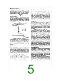
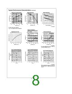
Ripple Rejection
Ripple rejection at the normal ripple frequency of 120 Hz is
a function of both electrical and thermal effects in the
LM196. If the adjustment pin is not bypassed with a capaci-
tor, it is also dependent on output voltage. A 25 mF capaci-
tor from the adjustment pin to ground will make ripple rejec-
tion independent of output voltage for frequencies above
100 Hz. If lower ripple frequencies are encountered, the ca-
pacitor should be increased proportionally.
A very important consideration is the size of the filter capac-
itor in the raw supply. At these high current levels, capacitor
size is usually dictated by ripple current ratings rather than
just obtaining a certain ripple voltage. Capacitor ripple cur-
rent (rms) is 2–3 times the DC output current of the filter. If
the capacitor has just 0.05X DC resistance, this can cause
30W internal power dissipation at 10A output current. Ca-
pacitor life is very sensitive to operating temperature, de-
To keep in mind that the bypass capacitor on the adjust-
ment pin will limit the turn-on time of the regulator. A 25 mF
capacitor, combined with the output divider resistance, will
give an extended output voltage settling time following the
application of input power.
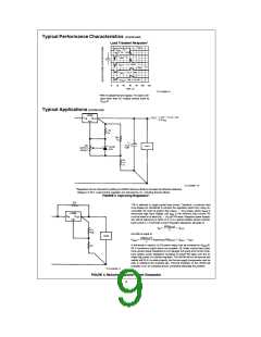
Load Regulation (LM196/LM396)
creasing by a factor of two for each 15 C rise in internal
§
Because the LM196 is a three-terminal device, it is not pos-
sible to provide true remote load sensing. Load regulation
will be limited by the resistance of the output pin and the
wire connecting the regulator to the load. For the data sheet
temperature. Since capacitor life is not all that great to start
with, it is obvious that a small capacitor with a large internal
temperature rise is inviting very short mean-time-to-failure.
A second consideration is the loss of usable input voltage to
the regulator. If the capacitor is small, the large dips in the
input voltage may cause the LM196 to drop out of regula-
tion. 2000 mF per ampere of load current is the minimum
recommended value, yielding about 2 Vp-p ripple of 120 Hz.
Larger values will have longer life and the reduced ripple will
allow lower DC input voltage to the regulator, with subse-
specification, regulation is measured 1/4 from the bottom
×
of the package on the output pin. Negative side sensing is a
true Kelvin connection, with the bottom of the output divider
returned to the negative side of the load.
4

 ETC [ ETC ]