INTERNAL TIME TAG
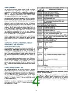
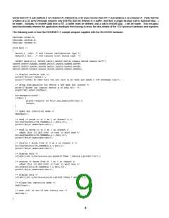
TABLE 3. COMMON MEMORY ADDRESS MAPPING
HEX DESCRIPTION/ACCESSIBILITY
The BU-65552, BU-65551 and BU-65550 include an internal
read/writable Time Tag Register. This register is a CPU
read/writable 16-bit counter with a programmable resolution of
either 2, 4, 8, 16, 32, or 64 µs per LSB. Another option allows the
Time Tag Register to be incremented under software control.
This supports self-test for the Time Tag Register.
ADDRESS
0000, 0001
0002, 0003
0004, 0005
0004, 0005
0006, 0007
0006, 0007
Interrupt Mask Register (RD/WR)
Configuration Register # 1 (RD/WR)
Configuration Register # 2 (RD/WR)
Configuration Register # 2 (RD/WR)
Start/Reset Register (WR)
For each message processed, the value of the Time Tag regis-
ter is loaded into the second location of the respective descrip-
tor stack entry ("TIME TAG WORD") for both BC and RT modes.
BC/RT Command Stack Pointer Register (RD)
BC Control Word/RT Subaddress Control Word
Register (RD/WR)
0008, 0009
Additional options are provided to clear the Time Tag Register
following a Synchronize (without data) mode command or load
the Time Tag Register following a Synchronize (with data) mode
command. Another option enables an interrupt request and a bit
in the Interrupt Status Register to be set when the Time Tag
Register rolls over from FFFF to 0000 (hex). Assuming the Time
Tag Register is not loaded or reset, this will occur at approxi-
mately 4-second time intervals, for 64 µs/LSB resolution, down
to 131 ms intervals, for 2 µs/LSB resolution.
000A, 000B Time Tag Register (RD/WR)
000C, 000D Interrupt Status Register (RD)
000E, 000F Configuration Register #3
0010, 0011
0012, 0013
0014, 0015
0016, 0017
0018, 0019
Configuration Register #4
Configuration Register #5
Data Stack Address Register (RD/WR)
BC Frame Time Remaining Register (RD)*
BC Time Remaining to Next Message Register (RD)*
Another programmable option for RT mode is for the Service
Request Status Word bit to be automatically cleared following
the PC Cards response to a Transmit Vector Word mode com-
mand.
BC Frame Time*/RT Last Command/MT Trigger Word*
Register (RD/WR)
001A,001B
001C, 001D RT Status Word Register (RD)
001E, 001F RT BIT Word Register (RD)
0020, 0021
•
•
•
Test Mode Register 0
ADDRESSING, INTERNAL REGISTERS, MEMORY
MANAGEMENT, AND INTERRUPTS
•
•
•
ADDRESSING THESE CARDS
002E,002F
Test Mode Register 7
All internal pointers used by these cards are assumed to be
word addresses, however byte addressing is used by the PC to
access memory and registers in the card. For example, to
access the the Area A Stack Pointer at word offset address 0100
(hex), a byte address offset of 0200 (hex) must be used (i.e. the
byte address is determined by multiplying the word address by
two).
0030, 0031
reserved
•
•
•
•
•
•
7FFE, 7FFF reserved
8000, 8001
12K x 16 Shared RAM (RD/WR) See NOTE below.
•
•
•
•
•
•
The shared RAM space starts at byte location 8000 if the mem-
ory allocation were contiguous. The registers are mapped into
memory locations 0X0000 through 0X002F. The memory
address space between 0X0030 and 0X7FFF is reserved. The
64K x 16 RAM uses page swapping, which is done in the device
driver.
DFFE, DFFF 12K x 16 Shared RAM (RD/WR)
E000, E001 reserved
•
•
•
•
•
•
FFFE, FFFF reserved
NOTES: 1. Normally RAM Addresses will be defined as an offset
from the base address
COMMON MEMORY ADDRESS MAP
2. BU-65551 shared RAM is 4K x 16
The software interface of the BU-65552, BU-65551 and BU-
65550 to the host processor consists of 17 internal operational
registers for normal operation, an additional 8 test registers, plus
shared memory (64K x 16 for BU-65552, 4K x 16 for BU-65551
and 12K x 16 for BU-65550). Both the registers and the shared
memory reside in the PCMCIA common memory space. See
TABLE 3. The BITMAPS of the 17 internal registers are shown
in TABLES 4 through 21.
Interrupt Mask Register: Used to enable and disable interrupt
requests for various conditions.
Configuration Registers #1 and #2: Used to select the PC
Cards mode of operation, and for software control of RT Status
Word bits, Active Memory Area, BC Stop-on-Error, RT Memory
Management mode selection, and control of the Time Tag oper-
ation.
Definition of the address mapping and accessibility for the BU-
65552, BU-65551 and BU-65550 17 nontest registers, and the
test registers, is as follows:
4

 ETC [ ETC ]