Page 8
Rev. 04/10/02
value of the input signal current. Some ac component
(at twice the input frequency) remains superimposed
on the dc output. The ac signal is attenuated by a
ripple alone.
2) The time constant of the 4301’s RMS detector is
determined by the combination of an external ca-
pacitor (connected to the CT pin) and an internal,
programmable current source. The current source
is equal to 1.1 IT. Normally, a resistor is not con-
nected directly to the CT pin on the 4301.
log-domain filter, which constitutes
a single-pole
rolloff with cutoff determined by an external capaci-
tor and a programmable dc current.
As in the VCA, input signals are currents to the
RMS IN pin. This input is a virtual ground, so a re-
sistor (R6 in Figure 2) is normally used to convert in-
put voltages to the desired current. The level detector
is capable of accurately resolving signals well below
10 mV (with a 10 kW input resistor). However, if the
detector is to accurately track such low-level signals,
ac coupling is normally required.
3) The 0 dB reference point, or level match, is not
adjustable via an external current source. However,
as in the 2252, the level match is affected by the
timing current, which, in this case, is drawn from
the IT pin and mirrored internally to CT.
4) The input stage of the 4301 RMS detector uses
integrated P-channel FETs rather than
a
The log-domain filter cutoff frequency is usually
placed well below the frequency range of interest. For
an audio-band detector, a typical value would be
5 Hz, or a 32 ms time constant (t). The filter’s time
constant is determined by an external capacitor at-
tached to the CT pin, and an internal current source
(ICT) connected to CT. The current source is pro-
grammed via the IT pin: current in IT is mirrored to
ICT with a gain of approximately 1.1. The resulting
time constant t is approximately equal to 0.026 CT/IT.
Note that, as a result of the mathematics of RMS de-
tection, the attack and release time constants are
fixed in their relationship to each other.
bias-current corrected bipolar differential amplifier.
Input bias currents are therefore negligible, improv-
ing performance at low signal levels.
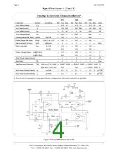
The Opamps — in Brief
The three opamps in the 4301 are intended for
general purpose applications. All are 5 MHz opamps
with slew rates of approximately 2V/ms. All use bipo-
lar PNP input stages. However, the design of each is
optimized for its expected use. Therefore, to get the
most out of the 4301, it is useful to know the major
differences among these opamps.
OA3, being internally connected to the output of
the VCA, is intended for current-to-voltage conver-
sion. Its input noise performance, at 7.5nV Hz, com-
The dc output of the detector is scaled with the
same constant of proportionality as the VCA gain
control: 6.5 mV/dB. The detector’s 0 dB reference
(Iin0, the input current which causes 0 V output), is
determined by IT as follows: Iin0= 9.6 mA It The de-
tector output stage is capable of sinking or sourcing
100 mA.
plements that of the VCA, adding negligible noise at
unity gain. Its output section is capable of driving a
2 kW load to within 2V of the power supply rails,
making it possible to use this opamp directly as the
output stage in single-ended designs.
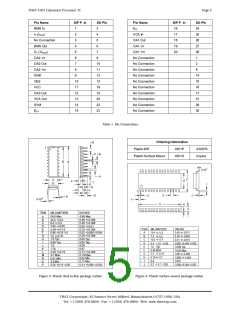
Differences between the 4301’s RMS-Level Detec-
tor circuitry and that of the THAT 2252 RMS Detec-
tor are as follows:
OA1 is the quietest opamp of the three. Its input
noise voltage, at 6.5nV Hz, makes it the opamp of
choice for input stages. Note that its output drive ca-
pability is limited (in order to reduce the chip’s
power dissipation) to approximately ±3 mA. It is
comfortable driving loads of 5 kW or more to within
1V of the power supply rails.
1) The rectifier in the 4301 RMS Detector is inter-
nally balanced by design, and cannot be balanced
via an external control. The 4301 will typically bal-
ance positive and negative halves of the input signal
within ±1.5%, but in extreme cases the mismatch
may reach ±15%. However, a 15% mismatch will
not significantly increase ripple-induced distortion
in dynamics processors over that caused by signal
OA2 is intended primarily as a control-voltage
processor. Its input noise parallels that of OA3, and
its output drive capability parallels that of OA1.
THAT Corporation; 45 Sumner Street; Milford, Massachusetts 01757-1656; USA
Tel: +1 (508) 478-9200; Fax: +1 (508) 478-0990; Web: www.thatcorp.com

 ETC [ ETC ]