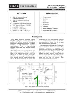
Page 4
Rev. 04/10/02
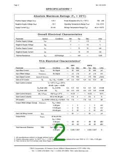
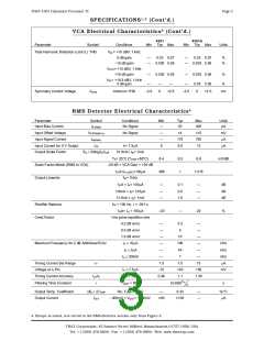
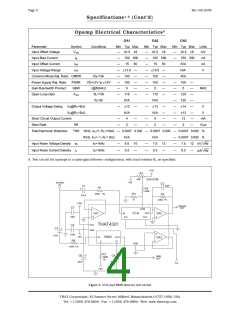
Specifications1,2 (Cont’d)
Opamp Electrical Characteristics5
OA1
OA2
OA3
Min Typ Max Units
Parameter
Symbol
VOS
Conditions
Min Typ Max
Min Typ Max
Input Offset Voltage
Input Bias Current
Input Offset Current
Input Voltage Range
—
—
—
—
—
—
—
—
±0.5 ±6
—
—
—
—
—
—
—
—
±0.5 ±6
—
—
±0.5 ±6
150 500
N/A
mV
nA
nA
V
IB
150 500
150 500
IOS
IVR
15
±13.5
100
100
5
50
—
—
—
—
—
15
±13.5
100
100
5
50
—
—
—
—
—
N/A
Common Mode Rej. Ratio CMRR
RS<10k
VS=±7V to ±15V
(@50kHz)
RL=10k
N/A
Power Supply Rej. Ratio
Gain Bandwidth Product
Open Loop Gain
PSRR
GBW
AVO
—
—
—
—
—
—
—
—
100
5
—
—
—
—
—
—
—
—
MHz
115
N/A
±13
N/A
4
110
N/A
±13
N/A
4
125
120
±14
±13
12
RL=2k
Output Voltage Swing VO@RL=5kW
VO@RL=2kW
—
—
—
—
—
—
—
V
V
Short Circuit Output Current
—
—
—
—
—
—
mA
V/ms
%
Slew Rate
SR
2
2
2
Total Harmonic Distortion
THD 1kHz, AV=1, RL=10kW — 0.0007 0.003 — 0.0007 0.003 — 0.0007 0.003
1kHz, AV=–1, RL= 2kW
N/A
N/A
— 0.0007 0.003
%
Input Noise Voltage Density en
Input Noise Current Density in
fO=1kHz
—
—
6.5 10
—
—
7.5 12
—
—
7.5 12 nV Hz
fO=1kHz
0.3
—
0.3
—
0.3
—
pA Hz
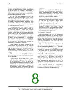
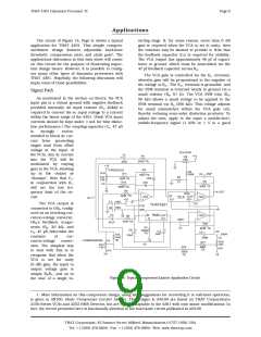
5. Test circuit for opamps is a unity-gain follower configuration, with load resistor RL as specified.
+15V
R5
50K
VCA SYM
-15V
SIGNAL
IN
C2
R2
47pF
C1
R1
R4
300K
20K0 1%
R3
47uF
51
1%
20K0
+15V
SIGNAL
OUT
C7
SYM
OUT
EC+
-
-
OA1
IN
EC-
VCA
OA3
100n
C8
+
+
VCC THAT4301
C3
VEE
+
OA2
-
100n
R6
47uF
-15V
IN
RMS OUT
Ct
It
GND
10K0 1%
R7
2M00
1%
C4
C6
RMS
OUT
10uF
22uF
Ec-
-15V
Figure 2. VCA and RMS detector test circuit
THAT Corporation; 45 Sumner Street; Milford, Massachusetts 01757-1656; USA
Tel: +1 (508) 478-9200; Fax: +1 (508) 478-0990; Web: www.thatcorp.com

 ETC [ ETC ]