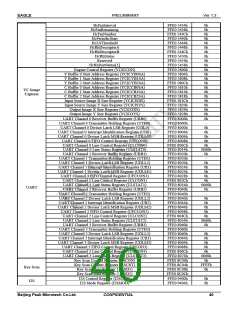
EAGLE
PRELIMINARY
Ver 1.3
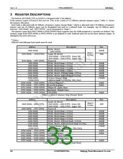
Peri-Block
Register Function
Address
Default Value
System ID Register (SYSID)
Configuration Register (CFG)
USB Host / Device Select Register (USBSEL)
FFE0 0000h
FFE0 0004h
FFE0 0008h
FFE0 0010h
FFE0 0014h
FFE0 0018h
FFE0 001Ch
FFE0 0020h
FFE0 0024h
FFE0 0028h
FFE0 002Ch
FFE0 0400h
FFE0 0404h
FFE0 0408h
FFE0 040Ch
FFE0 0410h
FFE0 0414h
FFE0 0418h
FFE0 041Ch
FFE0 0420h
FFE0 0424h
FFE0 0430h
FFE0 0434h
FFE0 0438h
FFF0 0800h
FFF0 0804h
FFF0 0808h
FFF0 080Ch
FFF0 0810h
FFF0 0818h
FFE0 0820h
FFE0 0824h
FFE0 0828h
FFE0 082Ch
FFE0 0830h
FFE0 0840h
FFE0 0844h
FFE0 0848h
FFE0 084Ch
FFE0 0850h
FFE0 0C00h
FFE0 0C04h
FFE0 0C08h
FFE0 0C0Ch
FFE0 0C10h
FFE0 0C14h
FFE0 0C18h
FFE0 0C1Ch
FFE0 0C20h
FFE0 0C24h
FFE0 0C28h
FFE0 0C2Ch
FFE0 0C30h
FFE0 0C34h
FFE0 0C38h
FFE0 0C40h
FFE0 1000h
0000 1A00h
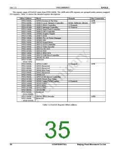
System
PinMux
0h
0h
0h
0h
0h
0h
0h
0h
0h
0h
FFF0h
FFF1h
FFF1h
FFF1h
FFF1h
FFF2h
FFF2h
7h
0h
00FFh
00F0h
3h
0h
0h
PinMux Control Register 0 (PINMUX0)
PinMux Control Register 1 (PINMUX1)
PinMux Control Register 2 (PINMUX2)
PinMux Control Register 3 (PINMUX3)
PinMux Control Register 4 (PINMUX4)
PinMux Control Register 5 (PINMUX5)
PinMux Control Register 6 (PINMUX6)
PinMux Control Register 7 (PINMUX7)
Local Memory Bank Control Register (MEMCON0)
Local Memory Bank Control Register (MEMCON1)
Local Memory Bank Control Register (MEMCON2)
Local Memory Bank Control Register (MEMCON3)
Local Memory Bank Control Register (MEMCON4)
Local Memory Bank Control Register (MEMCON5)
Local Memory Bank Control Register (MEMCON6)
Local SDRAM Clock Delay & Refresh Control (MEMCLKCON)
Frame Memory Area Start Address (FMASA)
1 MHz Frequency Generation Register (1MFREQGEN)
Texture Memory Control Register (TMEMCON)
Texture SDRAM Clock Delay & Refresh Control (TMEMCLKCON)
Texture Memory Area Start Address (TMASA)
DMA status register(GDMASTAT)
Local Memory
Controller
DMA interrupt mask register(GDMAIM)
0h
0h
DMA enable status register(GDMAESTAT)
DMA request status & synchronization register (GDMARSS)
DMA configuration register(GDMACFG)
0000 01E7h
0h
0h
0h
0h
0h
0h
0h
0h
0h
DMA last request register(GDMALR)
DMA Ch.0 Control Register(GDMACON0)
DMA Ch.0 Source Address Register(GDMAS0)
DMA Ch.0 Destination Address Register(GDMAD0)
DMA Ch.0 Transfer Count Register(GDMAT0)
DMA Ch.0 Descriptor Table Address Register(GDMADT0)
DMA Ch.1 Control Register(GDMACON1)
DMA Ch.1 Source Address Register(GDMAS1)
DMA Ch.1 Destination Address Register(GDMAD1)
DMA Ch.1 Transfer Count Register(GDMAT1)
DMA Ch.1 Descriptor Table Address Register(GDMADT1)
External Interrupt Source & Mode Select Register (INTMOD)
Interrupt Vector Register (INTVEC)
DMA
Controller
0h
0h
0h
00FF 0000h
0020h
Interrupt Vector Clear Register (INTVECCLR)
Interrupt Enable Register (INTEN)
0h
0h
0h
Interrupt Status Register (INTSTAT)
Interrupt Priority Programmable Register 0 (INPPR0)
Interrupt Priority Programmable Register 1 (INPPR1)
Interrupt Priority Programmable Register 2 (INPPR2)
Interrupt Priority Programmable Register 3 (INPPR3)
Interrupt Priority Programmable Register 4 (INPPR4)
Interrupt Priority Programmable Register 5 (INPPR5)
Interrupt Priority Programmable Register 6 (INPPR6)
Interrupt Priority Programmable Register 7 (INPPR7)
Interrupt Trigger Mode Programmable Register (IRQTRMD)
Interrupt Output Masking Register (INTMSK)
MCU Core Handshake Register (INTHSMCU)
NAND Flash Memory Control Register (NFMCON)
0302 0100h
0706 0504h
0B0A 0908h
0F0E 0D0Ch
1312 1110h
1716 1514h
1B1A 1918h
1F1E 1D1Ch
B980 DCFFh
FFFF FFFFh
0h
Interrupt
Controller
NAND Flash
0h
Beijing Peak Microtech Co.Ltd.
CONFIDENTIAL
36

 ETC [ ETC ]