Ver 1.3
PRELIMINARY
EAGLE
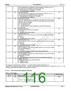
3.11.4.4 SDC Response Time Out Register (SDCRTO)
Address: FFE0 240Ch
Bit
31 : 8
7 : 0
R/W
R
R/W
Description
Default Value
Reserved
Response time out.
-
FFh
These bits configure the maximum waiting time for response. Response
time out error occurs if response is not received within the configured
time. Time unit is based on the transmitting clock.The clock counter starts
counting after the last command bit is transmitted.
01h : 1 clock count
02h : 2 clock counts
...
FFh : 255 clock counts
3.11.4.5 SDC Read Data Time Out Register (SDCRDTO)
Address: FFE0 2410h
Bit
31 : 16
15 : 8
R/W
R
R/W
Description
Default Value
Reserved
Data read time out.
-
FFh
These bits configure the maximum waiting time for receiving read data
starting from the transmission of read command.The upper 8 bits are
configurable by user while the lower 8 bits are fixed to 00h. The
recommended configuration is FF00h
7 : 0
R
Reserved
-
3.11.4.6 SDC Block Length Register (SDCBL)
Address: FFE0 2414h
Bit
31 : 12
11 : 0
R/W
R
R/W
Description
Default Value
Reserved
Block length.
-
200h
These bits configure the byte size of block which is the basic unit of data
transfer.
3.11.4.7 SDC Number of Block Register (SDCNOB)
Address: FFE0 2418h
Bit
31 : 16
15 : 0
R/W
R
R/W
Description
Default Value
Reserved
-
These bits defines the number of blocks allowed for transmission within a
multi-block command. This value should equal to ‘0’ at the end of
transmission. It decrements by one each time a block transmission
completes.
0000h
3.11.4.8 SDC Interrupt Enable Register (SDCIE)
Address : FFE0 241Ch
Bit
31 : 8
7
R/W
Description
Default Value
Reserved
-
0b
R/W
Card insert detection Interrupt enable
0 : disable
1 : enable
6
R/W
Card remove detection Interrupt enable
0b
0 : disable
1 : enable
117
CONFIDENTIAL
Beijing Peak Microtech Co.Ltd.

 ETC [ ETC ]