LHF80V25
25
sharp
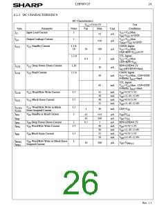
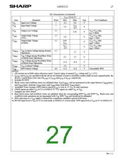
DC Characteristics (Continued)
V
=5V±0.5V
Max.
CC
Sym.
Parameter
Input Low Voltage
Input High Voltage
Notes
Min.
-0.5
Unit
V
Test Conditions
V
V
7
7
0.8
IL
V
+0.5
IH
CC
2.4
V
V
V
V
V
V
V
V
V
V
V
Output Low Voltage
3,7
3,7
3,7
V
I
=V Min.
OL
CC
CC
0.45
=5.8mA
OL
Output High Voltage
(TTL)
V
I
=V Min.
OH1
OH2
CC
CC
2.4
=-2.5mA
OH
Output High Voltage
(CMOS)
0.85
V
I
=V Min.
CC
CC
V
=-2.0mA
CC
OH
V
-0.4
V
I
=V Min.
CC
CC
CC
=-100µA
OH
V
V
V
V
Lockout Voltage during Normal
4,7
PPLK
PPH1
PPH2
PP
1.5
5.5
Operations
V
Voltage during Word/Byte Write
PP
4.5
or Block Erase Operations
V
Voltage during Word/Byte Write
PP
11.4
12.6
or Block Erase Operations
V
V
V
Lockout Voltage
2.0
V
V
LKO
CC
RP# Unlock Voltage
8,9
11.4
12.6
Unavailable WP#
HH
NOTES:
1. All currents are in RMS unless otherwise noted. Typical values at nominal V voltage and T =+25°C.
CC
A
2. I
and I
are specified with the device de-selected. If read or word/byte written while in erase suspend mode, the
CCWS
CCES
device’s current draw is the sum of I
3. Includes RY/BY#.
or I
and I
or I
, respectively.
CCWS
CCES
CCR
CCW
4. Block erases and word/byte writes are inhibited when V ≤V
, and not guaranteed in the range between V
(max.)
PP
PPLK
PPLK
and V
(min.), between V
(max.) and V
(min.) and above V
(max.).
PPH1
PPH1
PPH2
PPH2
5. Automatic Power Savings (APS) reduces typical I
to 1mA at 5V V in static operation.
CCR
CC
6. CMOS inputs are either V ±0.2V or GND±0.2V. TTL inputs are either V or V .
CC
IL
IH
7. Sampled, not 100% tested.
8. Boot block erases and word/byte writes are inhibited when the corresponding RP#=V and WP#=V . Block erase and
IH
IL
word/byte write operations are not guaranteed with V <RP#<V and should not be attempted.
IH
HH
9. RP# connection to a V supply is allowed for a maximum cumulative period of 80 hours.
HH
10. BYTE# input level is V ±0.2V in word mode or GND±0.2V in byte mode. WP# input level is V ±0.2V or GND±0.2V.
CC
CC
Rev. 1.2

 ETC [ ETC ]