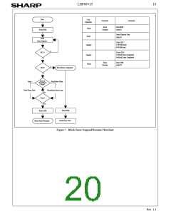
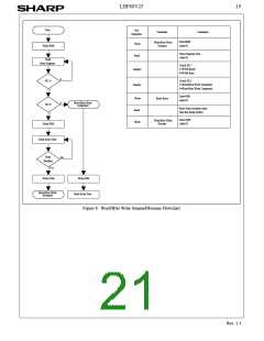
LHF80V25
22
sharp
*WARNING: Stressing the device beyond the "Absolute
Maximum Ratings" may cause permanent damage. These
are stress ratings only. Operation beyond the "Operating
Conditions" is not recommended and extended exposure
beyond the "Operating Conditions" may affect device
reliability.
6 ELECTRICAL SPECIFICATIONS
6.1 Absolute Maximum Ratings*
Operating Temperature
During Read, Block Erase and
Word/Byte Write.................................0°C to +70°C
(1)
NOTES:
Temperature under Bias...................... -10°C to +80°C
Storage Temperature ................................ -65°C to +125°C
Voltage On Any Pin
1. Operating temperature is for commercial temperature
product defined by this specification.
2. All specified voltages are with respect to GND.
Minimum DC voltage is -0.5V on input/output pins
and -0.2V on V and V pins. During transitions,
(2)
CC
PP
(except V , V , and RP#) ............ -0.5V to +7.0V
CC
PP
this level may undershoot to -2.0V for periods <20ns.
Maximum DC voltage on input/output pins and V is
(2)
CC
V
V
Supply Voltage................................ -0.2V to +7.0V
CC
V
V
+0.5V which, during transitions, may overshoot to
+2.0V for periods <20ns.
CC
CC
Update Voltage during Block
Erase and Word/Byte Write .........-0.2V to +14.0V
PP
3. Maximum DC voltage on V and RP# may overshoot
(2,3)
(2,3)
(4)
PP
to +14.0V for periods <20ns.
4. Output shorted for no more than one second. No more
than one output shorted at a time.
RP# Voltage ........................................-0.5V to +14.0V
Output Short Circuit Current................................100mA
6.2 Operating Conditions
Temperature and V Operating Conditions
CC
Symbol
Parameter
Min.
Max.
+70
5.5
Unit
°C
Test Condition
T
Operating Temperature
0
Ambient Temperature
A
V
V
Supply Voltage (4.5V-5.5V)
4.5
V
CC
CC
(1)
6.2.1 CAPACITANCE
T =+25°C, f=1MHz
A
Symbol
Parameter
Typ.
Max.
Unit
Condition
C
C
Input Capacitance
Output Capacitance
7
9
10
12
pF
pF
V =0.0V
IN
OUT
IN
V
=0.0V
OUT
NOTE:
1. Sampled, not 100% tested.
Rev. 1.2

 ETC [ ETC ]