LHF80V25
20
sharp
5 DESIGN CONSIDERATIONS
5.1 Three-Line Output Control
5.3 Power Supply Decoupling
Flash memory power switching characteristics require
careful device decoupling. System designers are interested
in three supply current issues; standby current levels,
active current levels and transient peaks produced by
falling and rising edges of CE# and OE#. Transient current
magnitudes depend on the device outputs’ capacitive and
inductive loading. Two-line control and proper decoupling
capacitor selection will suppress transient voltage peaks.
Each device should have a 0.1µF ceramic capacitor
connected between its V and GND and between its V
The device will often be used in large memory arrays.
SHARP provides three control inputs to accommodate
multiple memory connections. Three-line control provides
for:
a. Lowest possible memory power dissipation.
b. Complete assurance that data bus contention will not
occur.
CC
PP
and GND. These high-frequency, low inductance
capacitors should be placed as close as possible to package
leads. Additionally, for every eight devices, a 4.7µF
electrolytic capacitor should be placed at the array’s power
To use these control inputs efficiently, an address decoder
should enable CE# while OE# should be connected to all
memory devices and the system’s READ# control line.
This assures that only selected memory devices have
active outputs while deselected memory devices are in
standby mode. RP# should be connected to the system
POWERGOOD signal to prevent unintended writes during
system power transitions. POWERGOOD should also
toggle during system reset.
supply connection between V
and GND. The bulk
CC
capacitor will overcome voltage slumps caused by PC
board trace inductance.
5.4 V Trace on Printed Circuit Boards
PP
Updating flash memories that reside in the target system
requires that the printed circuit board designer pay
attention to the V Power supply trace. The V pin
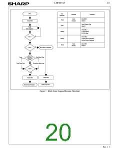
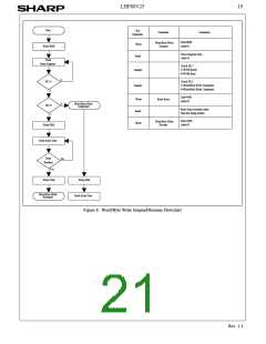
5.2 RY/BY#, Block Erase and Word/Byte
Write Polling
PP
PP
supplies the memory cell current for word/byte writing
and block erasing. Use similar trace widths and layout
considerations given to the V power bus. Adequate V
RY/BY# is an open drain output that should be connected
CC
PP
to V by a pull up resistor to provide a hardware method
CC
supply traces and decoupling will decrease V voltage
PP
of detecting block erase and word/byte write completion.
It transitions low after block erase or word/byte write
commands and returns to High Z when the WSM has
finished executing the internal algorithm.
spikes and overshoots.
RY/BY# can be connected to an interrupt input of the
system CPU or controller. It is active at all times. RY/BY#
is also High Z when the device is in block erase suspend
(with word/byte write inactive), word/byte write suspend
or deep power-down modes.
Rev. 1.2

 ETC [ ETC ]