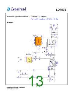
LD7575
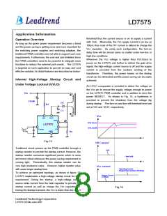
Current Sensing, Leading-edge Blanking and
the Negative Spike on CS Pin
The typical current mode PWM controller feedbacks both
current signal and voltage signal to close the control loop
and achieve regulation. The LD7575 detects the primary
MOSFET current from the CS pin, which is not only for the
peak current mode control but also for the pulse-by-pulse
current limit. The maximum voltage threshold of the current
sensing pin is set as 0.85V. Thus the MOSFET peak current
can be calculated as:
0.85V
I
=
PEAK(MAX)
R
S
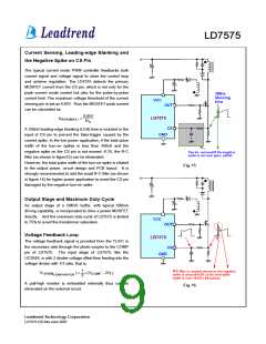
A 350nS leading-edge blanking (LEB) time is included in the
input of CS pin to prevent the false-trigger caused by the
current spike. In the low power application, if the total pulse
width of the turn-on spikes is less than 350nS and the
negative spike on the CS pin is not exceed -0.3V, the R-C
filter (as shown in figure15) can be eliminated.
However, the total pulse width of the turn-on spike is related
to the output power, circuit design and PCB layout. It is
strongly recommended to add the small R-C filter (as shown
in figure 16) for higher power application to avoid the CS pin
damaged by the negative turn-on spike.
Fig. 15
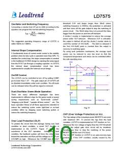
Output Stage and Maximum Duty-Cycle
An output stage of a CMOS buffer, with typical 500mA
driving capability, is incorporated to drive a power MOSFET
directly. And the maximum duty-cycle of LD7575 is limited
to 75% to avoid the transformer saturation.
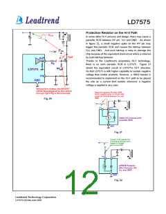
Voltage Feedback Loop
The voltage feedback signal is provided from the TL431 in
the secondary side through the photo-coupler to the COMP
pin of LD7575. The input stage of LD7575, like the
UC384X, is with 2 diodes voltage offset then feeding into the
voltage divider with 1/3 ratio, that is,
1
V
COMPARATOR ) = × (V
− 2V )
+(PWM
COMP F
3
A pull-high resistor is embedded internally thus can be
eliminated on the external circuit.
Fig. 16
9
Leadtrend Technology Corporation
LD7575-DS-04a June 2007

 ETC [ ETC ]