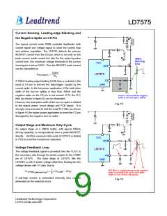
LD7575
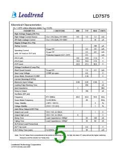
Electrical Characteristics
(TA = +25oC unless otherwise stated, VCC=15.0V)
PARAMETER
CONDITIONS
MIN
TYP
MAX
UNITS
High-Voltage Supply (HV Pin)
High-Voltage Current Source
Off-State Leakage Current
Supply Voltage (Vcc Pin)
Startup Current
Vcc< UVLO(on), HV=500V
Vcc> UVLO(off), HV=500V
0.5
1.0
1.5
35
mA
µA
100
3.0
4.0
µA
mA
mA
mA
V
VCOMP=0V
2.0
2.5
Operating Current
VCOMP=3V
(with 1nF load on OUT pin)
Protection tripped (OLP, OVP)
0.5
UVLO (off)
9.0
10.0
16.0
27.5
11.0
17.0
30.0
UVLO (on)
15.0
25.0
V
OVP Level
V
Voltage Feedback (Comp Pin)
Short Circuit Current
Open Loop Voltage
Green Mode Threshold VCOMP
Current Sensing (CS Pin)
Maximum Input Voltage
Leading Edge Blanking Time
Input impedance
VCOMP=0V
1.5
6.0
2.2
mA
V
COMP pin open
2.35
V
0.80
1
0.85
350
0.90
V
nS
MΩ
nS
Delay to Output
100
Oscillator (RT pin)
Frequency
RT=100KΩ
60.0
65.0
20
70.0
KHz
KHz
%
Green Mode Frequency
Temp. Stability
Fs=65.0KHz
(-40°C ~105°C)
(VCC=11V-25V)
3
1
Voltage Stability
%
Gate Drive Output (OUT Pin)
Output Low Level
VCC=15V, Io=20mA
1
V
V
Output High Level
Rising Time
VCC=15V, Io=20mA
9
Load Capacitance=1000pF
Load Capacitance=1000pF
50
30
160
60
nS
nS
Falling Time
OLP (Over Load Protection)
OLP Trip Level
5.0
30
V
OLP Delay Time (note)
Fs=65KHz
mS
Note: The OLP delay time is proportional to the period of switching cycle. So that, the lower RT value will set the higher switching
frequency and the shorter OLP delay time.
5
Leadtrend Technology Corporation
LD7575-DS-04a June 2007

 ETC [ ETC ]