1-2-1 2-Phase Stepper Motor Unipolar Driver ICs
SLA7031M/SLA7032M/SLA7033M 2-Phase/1-2 Phase Excitation
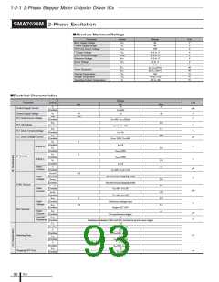
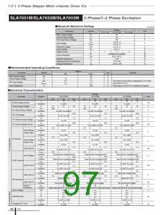
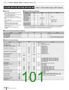
■Absolute Maximum Ratings
(Ta=25°C)
Ratings
Parameter
Symbol
Unit
SLA7031M
SLA7032M
46
SLA7033M
Motor Supply Voltage
VCC
V
V
V
Control Supply Voltage
FET Drain-Source Voltage
VS
46
V
DSS
IN
SYNC
REF
100
V
–0.3 to +7
–0.3 to +7
–0.3 to +7
–5 to +7
1.5
Input Voltage
V
V
Reference Voltage
Sense Voltage
Output Current
V
V
V
V
RS
IO
1
3
A
P
D1
D2
4.5(Without Heatsink)
35(T =25°C)
W
W
°C
°C
°C
Power Dissipation
P
c
Channel Temperature
T
ch
+150
Operating Ambient Temperature
Storage Temperature
T
a
–20 to+85
–40 to +150
Tstg
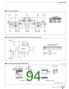
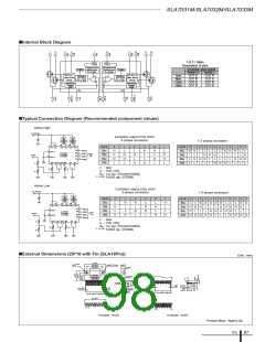
■Recommended Operating Conditions
Ratings
Parameter
Symbol
Unit
Remarks
min.
max.
44
Motor Supply Voltage
Control Supply Voltage
V
M
V
V
VS
10
0.1
4.0
44
The control current precision is degraded at 0.1V or lower.
Output MOS FET OFF
VREF
1.0
5.5
100
V
REF Input Voltage
Case Temperature
VREF(dis)
V
Temperature of 4(15)-Pin Lead(without heatsink)
TC
°C
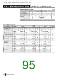
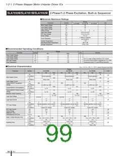
■Electrical Characteristics
Ratings
Parameter
Symbol
SLA7031M
SLA7032M
SLA7033M
Unit
min.
typ.
10
max.
min.
typ.
10
max.
min.
typ.
10
max.
15
I
S
15
15
Control Supply Current
Control Supply Voltage
FET Drain-Source Voltage
mA
V
Condition
V
S
=44V
24
V
S
=44V
V
S
=44V
24
V
S
10
44
10
24
44
10
44
VDSS
100
100
100
V
Condition
V
S
=44V, IDSS=250µA
VS
=44V, IDSS=250µA
VS=44V, IDSS=250µA
V
DS
0.85
1.2
0.6
1.1
250
0.85
2.3
FET ON Voltage
V
V
Condition
I
D
=1A, V
S
=10V
I
D
=1A, V
S
=14V
ID=3A, VS=14V
VSD
FET Diode Forward Voltage
FET Drain Leakage Current
Condition
I
SD=1A
I
SD=1A
ISD=3A
IDSS
250
250
µA
Condition
V
DSS=100V, V
S=44V
V
DSS=100V, V
S=44V
VDSS=100V, VS=44V
V
IH
2.0
2.0
2.0
2.0
2.0
2.0
Input Voltage
(Active High)
Condition
I
D
=1A
I
D
=1A
ID=3A
V
V
IL
0.8
0.8
0.8
Condition
V
V
DSS=100V
DSS=100V
V
DSS=100V
DSS=100V
V
DSS=100V
DSS=100V
V
IH
IN Terminal
Input Voltage
Condition
V
V
V
µA
V
(Active Low)
V
IL
0.8
0.8
0.8
Condition
I
D
=1A
I
D
=1A
ID=3A
I
I
±1
±1
±1
Input Current
Condition
VS
=44V, V
I=0 or 5V
V
S
=44V, V
I=0 or 5V
VS=44V, VI=0 or 5V
VSYNC
4.0
4.0
4.0
Condition
Synchronous chopping mode
Synchronous chopping mode
Synchronous chopping mode
Input Voltage
SYNC Terminal
VSYNC
0.8
Asynchronous chopping mode
0.1
0.8
Asynchronous chopping mode
0.1
0.8
Asynchronous chopping mode
0.1
Condition
I
SYNC
Condition
V
S
=44V, VSYNC=5V
V
S
=44V, VSYNC=5V
V
S
=44V, VSYNC=5V
Input Current
mA
I
SYNC
–0.1
2.0
–0.1
2.0
–0.1
2.0
Condition
V
S=44V, VSYNC=0V
VS
=44V, VSYNC=0V
VS
=44V, VSYNC=0V
VREF
0
0
0
Condition
Reference Voltage input
Reference Voltage input
Reference Voltage input
Input Current
V
VREF
4.0
5.5
4.0
5.5
4.0
5.5
Condition
Output FET OFF
Output FET OFF
Output FET OFF
REF Terminal
Input Current
I
REF
±1
±1
±1
µA
Condition
No synchronous trigger
40
No synchronous trigger
40
No synchronous trigger
40
RREF
Internal
Ω
Resistance
Condition
VR
Resistance between GND and REF terminal at synchronous trigger
REF
Resistance between GND and REF terminal at synchronous trigger
REF
Resistance between GND and REF terminal at synchronous trigger
REF
Sense Voltage
Switching Time
S
V
V
V
V
T
r
0.5
0.7
0.1
0.5
0.7
0.5
0.7
Tstg
µs
µs
T
f
0.1
0.1
Condition
VS
=24V, I
D
=0.8A
V
S
=24V, I
D=1A
V
S
=24V, I
D=1A
T
OFF
12
12
12
Chopping OFF Time
Condition
V
S
=24V
V
S=24V
VS=24V
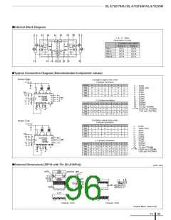
ICs
96

 ETC [ ETC ]