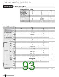
SMA7036M
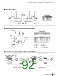
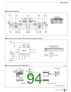
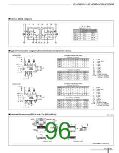
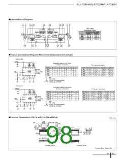
■Internal Block Diagram
1
6
5
8
14
10
15
1, 6, 10, 15pin
Description of pins
Excitation input signal
Reg.
Reg.
Active H
OUT A
OUT A
OUT B
OUT B
Active L
OUT A
OUT A
OUT B
OUT B
1pin
6pin
10pin
15pin
Chopping noise
blanking timer
Chopping noise
blanking timer
Oscillator
Oscillator
µ
µ
(5 s typ)
(5 s typ)
MOSFET
gate drive
circuit
MOSFET
gate drive
circuit
Chopping
OFF timer
Chopping
OFF timer
µ
(12 s typ)
+
–
+
–
(12
µ
s typ)
Synchronous
chopping
circuit
Synchronous
chopping
circuit
7
2
4
3
13
12
11
9
■Typical Connection Diagram (Recommended component values)
Vcc (46V max)
+
Excitation signal time chart
2-phase excitation
8
1
6
10
15
V
S
clock
0
H
L
1
H
H
2
L
3
L
L
0
1
H
H
2
5
IN
IN
A
B
IN
A
B
Sync
Sync
A
IN
IN
A
H
L
SMA7036M
B
H
Vb (5V)
11
14
B
IN
r
r
1
: 8kΩ
r1
PchMOS
2
: 2kΩ (VR)
Rs
A
Ref
A
Ref
13
B
Rs
B
G
A
GB
7
3
9
4
12
RS (1 to 2W) : 1Ω typ
PchMOS
Inv
: HN1J02FU (Toshiba)
: 7404
Rs
Rs
r2
Inv
Disable (High Active)
■External Dimensions (ZIP15 [SMA15Pin])
(Unit : mm)
Epoxy resin package
4±0.2
31±0.2
2.5±0.2
Lot No.
Part No.
1.45±0.15
0.62±0.1
1.16±0.15
1.2±0.1
(5.9)
+0.2
–0.1
+0.2
–0.1
+0.2
0.65
1.16
0.55
–0.1
(7.5)
P2.03±0.1×14=28.42
4±0.7
P2.03±0.1×14=28.42
31.3+0.2
.
. . . . . . .
15
1 2 3
.
. . . . . .
15
123
Forming No. No.1054
Forming No. No.1055
Product Mass : Approx.4g
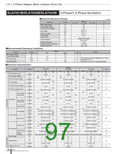
ICs
93

 ETC [ ETC ]