SLA7050M/SLA7051M/SLA7052M
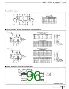
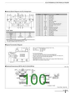
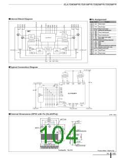
■Internal Block Diagram and Pin Assignment
Pin No.
Symbol
Function
1
2
OutA
NC
Phase A output
No Connection
Phase A output
No Connection
Logic supply
1
2
3
4
11 12
14
Reg
7
5
15
16
17
18
MIC
3
OutA/
GA
GA
GB
4
Sequencer
GA/
GB/
5
VCC
OSC
OSC
6
SenseA
Clock
Phase A current sense
Step Clock input
PWM
Control
Synchro
Control
PWM
Control
7
8
Sync
Synchronous PWM control signal input
Control current setting & output OFF
Device GND
Sleep
Circuit
9
Ref
10
11
12
13
14
15
16
17
18
GND
CW/CCW
Full/Half
SenseB
Normal/reverse control input
Full/Half Step control input
Phase B current sense
Load supply (motor supply)
No Connection
6
9
8
10
13
V
S
Truth Table
GB
OutB/
NC
L
H
Phase B output
CW/CCW
Full/Half
REF
CW
CCW
Half
No Connection
Full
OutB
Phase B output
Enable
Disable
Sync
Asynchronous
Synchronous
Clock
* REF terminal turns into normal operation at VREF < 1.5V.
The output is disabled (Output OFF) at VREF > 2V.
■Typical Connection Diagram
.
Rs=0.1 to 2Ω (Power dissipation should be: P IO2 × RS)
=
.
Vs=10~44V
CA
R1=10kΩ
CA=100µF/50V
R2=5.1kΩ (VR) CB=10µF/10V
Q1:T.B.D
1
3
2
4
14
15
17 16 18
Vcc=3.0~5.5V
Disable
5
7
Vcc
r1
* VCC line noise precaution:
Q1
CB
SLA7050M
SLA7051M
SLA7052M
The device may malfunction if the VCC line noise exceeds 0.5V.
* Be sure to connect the unused logic input terminals (CW/CCW, F/H, Sync) to VCC
or GND. If they are open, the device will malfunction.
* GND pattern precaution:
Clock
Micro-
computer,
etc.
11
12
8
CW/CCW
Full/Half
Sync
9
REF
Separating the VCC system GND (S-GND) and VS system GND (P-GND) from the
device GND (10-Pin) helps to reduce noise.
6
13
10
r2
RsA
RsB
P-GND
S-GND
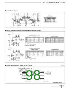
■External Dimensions (ZIP18 with Fin [SLA18Pin])
(Unit : mm)
31±0.2
24.4±0.2
16.4±0.2
φ3.2±0.15
φ3.2±0.15×3.8 4.8±0.2
1.7±0.1
Part Number
Lot No.
2.45±0.2
R-End
+0.2
–0.1
+0.2
–0.1
0.65
2.2±0.6
1
+0.2
–0.1
+0.2
+0.2
6±0.6
0.65
1
–0.1
0.55
4±0.7
–0.1
7.5±0.6
17×P1.68±0.4=28.56±1
17×P1.68±0.4=28.56±1
31.3±0.2
.
. . . . . .
.
. . . . . .
123
18
1 2 3
18
Forming No. No.871
Forming No. No.872
Product Mass : Approx.6g
ICs
99

 ETC [ ETC ]