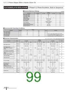
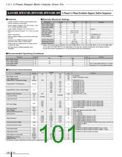
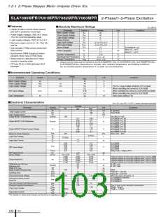
1-2-1 2-Phase Stepper Motor Unipolar Driver ICs
SLA7050M/SLA7051M/SLA7052M 2-Phase/1-2 Phase Excitation, Built-in Sequencer
■Absolute Maximum Ratings
(Ta=25°C)
Ratings
SLA7051M
46
Parameter
Symbol
Unit
SLA7050M
SLA7052M
Motor Supply Voltage
Load Supply Voltage
Logic Supply Voltage
Output Current
VM
VS
V
V
46
VCC
IO
6
V
1
2
3
A
Logic Input Voltage
REF Input Voltage
Sense Voltage
VIN
VREF
VRS
PD1
PD2
Tj
–0.3 to VCC+0.3
–0.3 to VCC+0.3
–2 to +2
V
V
V
4 (Without Heatsink)
20 (TC=25°C)
+150
W
W
°C
°C
°C
Power Dissipation
Junction Temperature
Operating Ambient Temperature
Storage Temperature
Ta
–20 to +85
–30 to +150
Tstg
■Recommended Operating Conditions
Ratings
Parameter
Symbol
Unit
Remarks
min.
max.
Motor Supply Voltage
VM
VS
44
44
V
V
Load Supply Voltage
Logic Supply Voltage
REF Input Voltage
Case Temperature
10
3.0
0.1
VCC
VREF
TC
5.5
1.0
100
V
V
The VCC surge voltage should be 0.5V or lower.
The control current precision is degraded at 0.1V or lower.
Temperature at pin-10 Lead (Without heatsink)
°C
■Electrical Characteristics
(VCC = 5V, VS = 24V, Ta = 25°C, unless otherwise specified)
Ratings
SLA7051M
typ.
Parameter
Symbol
SLA7050M
typ.
SLA7052M
typ.
Unit
min.
100
max.
15
min.
100
max.
15
min.
max.
15
ISS
mA
Conditions
IS
Normal operation
Sleep mode
Normal operation
Sleep mode
Normal operation
Sleep mode
Main Supply Current
Logic Supply Current
100
3
100
3
100
3
µA
Conditions
ICC
mA
V
Output MOSFET Breakdown
Voltage
VDSS
100
Conditions
RDS (ON)
Conditions
VSD
VS
=44V, IDSS=1mA
V
S
=44V, IDSS=1mA
VS=44V, IDSS=1mA
0.85
1.2
0.5
1.1
0.27
2.3
Ω
Output MOSFET ON Resistance
ID
=1A
I
D=1A
ID=3A
Output MOSFET Diode Forward
Voltage
V
Conditions
Fclock
I
SD=1A
I
SD=1A
ISD=3A
Maximum Clock Frequency
100
100
100
kHz
V
VIL
V
CC·0.25
V
CC·0.25
V
CC·0.25
Logic Input Voltage
VIH
V
CC·0.75
V
CC·0.75
V
CC·0.75
0
IIL
±1
±1
±1
±1
±1
±1
µA
Logic Input Current
REF Input Voltage
IIH
VREF
0
1.5
0
1.5
1.5
Conditions
VREFS
Normal-operation current control
Normal-operation current control
Normal-operation current control
V
2
VCC
2
V
CC
2
VCC
Conditions
IREF
Output OFF (sleep)
Output OFF (sleep)
Output OFF (sleep)
REF Input Current
Sense Voltage
±10
±10
±10
µA
V
VRS
VREF
VREF
VREF
PWM OFF Time
TOFF
12
12
12
µS
PWM Minimum ON Time
TON (min)
TSE
5
5
5
µS
µS
100
100
100
Sleep - Enable Recovery Time
Switching Time
Conditions
TONC
V
REF : 2.0→1.5V, I
O
: 0.75A
V
REF : 2.0→1.5V, I
O
: 1.5A
V
REF : 2.0→1.5V, IO : 2.0A
2.5
2.5
2.5
Conditions
TOFFC
Clock→Out
2.0
Clock→Out
2.0
Clock→Out
2.0
µS
Conditions
Clock→Out
Clock→Out
Clock→Out
ICs
98

 ETC [ ETC ]