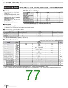
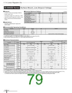
SI-3000ZD Series
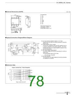
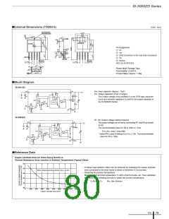
■External Dimensions (TO263-5)
(Unit : mm)
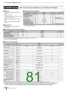
Case temperature
measurement point
0.2
10.0
(8.0)
(4.4)
(15°)
0.2
4.5
+0.10
–0.05
1.3
3-R0.3
0.2
(2×R0.45)
(3°)
φ1.5 Dp:
Pin Assignment
q VC
0.15
0.10
(3°)
(3°)
0.2
2.4
(R0.3)
w VIN
e GND (Common to the rear side of product)
0.10
0.25
0.88
(1.7
(R0.3)
0~6°
r VO
(0.5)
0.1
0.1
0.8
(1.7
t Sense
0.8
(1.7
0.25
0.25
0.25
)
(1.7
)
)
)
(ADJ for SI-3011ZD)
1
2
3
4
5
0.2
9.9
(3°)
(3°)
Plastic Mold Package Type
Flammability: UL94V-0
2-R0.3
0.1
0.02
10.0
Product Mass: Approx. 1.48g
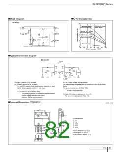
■Block Diagram
SI-3011ZD
V
IN
V
O
CIN: Input capacitor (Approx. 10µF)
2
4
5
+
CO: Output capacitor (47µF or larger)
*
R3
R1
C
IN
The output voltage may oscillate if a low ESR type capacitor
(such as a ceramic capacitor) is used for the output capacitor in
the SI-3000ZD Series.
+
+
-
Drive
OCP
REF
ADJ
TSD
CO
AMP1
+
ON/
OFF
-
R2
V
C
1
-
+
3
GND
SI-3033ZD
R1, R2: Output voltage setting resistors
The output voltage can be set by connecting R1 and R2 as shown
at left.
V
IN
V
4
O
2
+
5
CIN
SENSE
The recommended value for R2 is 10kΩ or 11kΩ.
+
+
Drive
OCP
REF
R1= (VO–VADJ) / (VADJ/R2)
-
CO
TSD
AMP1
+
*:Insert R3 in case of setting VO to VO ≤ 1.8V. The recommended
value for R3 is 10kΩ.
ON/
OFF
-
VC
1
-
+
3
GND
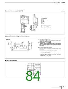
■Reference Data
Copper Laminate Area (on Glass-Epoxy Board) vs.
Thermal Resistance (from Junction to Ambient Temperature) (Typical Value)
55
• A higher heat radiation effect can be achieved by enlarging the copper laminate
area connected to the inner frame to which a monolithic IC is mounted.
• Obtaining the junction temperature
50
45
40
35
30
When Using Glass-Epoxy Board of 40 × 40 mm
θ
Measure GND terminal temperature TC with a thermocouple, etc. Then substitute
this value in the following formula to obtain the junction temperature.
Tj=PD×θj–C+TC
PD= (VIN–VO)•IOUT
0
200
400
600
800
1000 1200 1400 1600 1800
Copper Laminate Area (mm2)
ICs
79

 ETC [ ETC ]