ST90158 - I/O PORTS
PORT CONTROL REGISTERS (Cont’d)
During Reset, ports with weak pull-ups are set in
bidirectional/weak pull-up mode and the output
Data Register is set to FFh. This condition is also
held after Reset, except for Ports 0 and 1 in ROM-
less devices, and can be redefined under software
control.
Each pin of an I/O port may assume software pro-
grammable Alternate Functions (refer to the de-
vice Pin Description and to Section 8.5 ALTER-
NATE FUNCTION ARCHITECTURE). To output
signals from the ST9 peripherals, the port must be
configured as AF OUT. On ST9 devices with A/D
Converter(s), configure the ports used for analog
inputs as AF IN.
Bidirectional ports without weak pull-ups are set in
high impedance during reset. To ensure proper
levels during reset, these ports must be externally
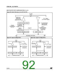
The basic structure of the bit Px.n of a general pur-
pose port Px is shown in Figure 50.
connected to either V
pull-up or pull-down resistors.
or V through external
DD
SS
Independently of the chosen configuration, when
the user addresses the port as the destination reg-
ister of an instruction, the port is written to and the
data is transferred from the internal Data Bus to
the Output Master Latches. When the port is ad-
dressed as the source register of an instruction,
the port is read and the data (stored in the Input
Latch) is transferred to the internal Data Bus.
Other reset conditions may apply in specific ST9
devices.
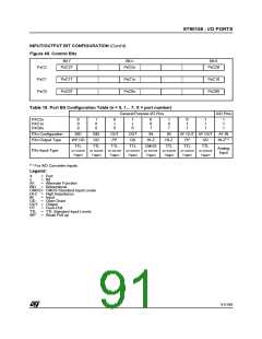
8.4 INPUT/OUTPUT BIT CONFIGURATION
By programming the control bits PxC0.n and
PxC1.n (see Figure 49) it is possible to configure
bit Px.n as Input, Output, Bidirectional or Alternate
Function Output, where X is the number of the I/O
port, and n the bit within the port (n = 0 to 7).
When Px.n is programmed as an Input:
(See Figure 51).
When programmed as input, it is possible to select
the input level as TTL or CMOS compatible by pro-
gramming the relevant PxC2.n control bit, except
where the Schmitt trigger option is assigned to the
pin.
– The Output Buffer is forced tristate.
– The data present on the I/O pin is sampled into
the Input Latch at the beginning of each instruc-
tion execution.
– The data stored in the Output Master Latch is
copied into the Output Slave Latch at the end of
the execution of each instruction. Thus, if bit Px.n
is reconfigured as an Output or Bidirectional, the
data stored in the Output Slave Latch will be re-
flected on the I/O pin.
The output buffer can be programmed as push-
pull or open-drain.
A weak pull-up configuration can be used to avoid
external pull-ups when programmed as bidirec-
tional (except where the weak pull-up option has
been permanently disabled in the pin hardware as-
signment).
90/199
9

 ETC [ ETC ]