ST90158 - ELECTRICAL CHARACTERISTICS
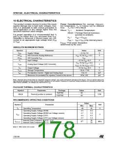
10 ELECTRICAL CHARACTERISTICS
This product contains devices to protect the inputs
against damage due to high static voltages, how-
ever it is advisable to take normal precaution to
avoid application of any voltage higher than the
specified maximum rated voltages.
Power Considerations.The average chip-junc-
tion temperature, T , in Celsius can be obtained
J
from:
T =TA + PD x RthJA
J
Where: T =
Ambient Temperature.
A
RthJA = Package thermal resistance
(junction-to ambient).
For proper operation it is recommended that V
I
.
and V be higher than V
and lower than V
O
SS
DD
P =
P
I
+ P
.
D
INT
PORT
Reliability is enhanced if unused inputs are con-
nected to an appropriate logic voltage level (V
P
=
x V (chip internal power).
DD
INT
DD
DD
or V ).
SS
P
=Port power dissipation
PORT
determined by the user)
ABSOLUTE MAXIMUM RATINGS
Symbol
Parameter
Value
– 0.3 to 7.0
-0.3 to V + 0.3
Unit
V
V
Supply Voltage
A/D Converter Analog Reference
DD
AV
AV
V
V
DD
SS
DD
DD
A/D Converter V
Input Voltage
V
SS
SS
V
– 0.3 to V +0.3
V
V
I
DD
V
-0.3 to V + 0.3
DD
SS
V
Analog Input Voltage (A/D Converter)
AIN
V
-0.3 to V
+ 0.3
SSA
DDA
V
Output Voltage
– 0.3 to V +0.3
V
O
DD
T
I
Storage Temperature
– 55 to + 150
-5 to +5
°C
STG
INJ
Pin Injection Current Digital and Analog Input
Maximum Accumulated Pin injection Current in the device
mA
mA
-50 to +50
Note: Stresses above those listed as “absolute maximum ratings“ may cause permanent damage to the device. This is a stress rating only
and functional operation of the device at these conditions is not implied. Exposure to maximum rating conditions for extended periods may
affect device reliability. All voltages are referenced to V
SS
PACKAGE THERMAL CHARACTERISTICS
Symbol
Parameter
Package
TQFP80
PQFP80
Value
40
Unit
RthJA
Thermal junction to ambient
°C/W
40
RECOMMENDED OPERATING CONDITIONS
Value
Symbol
Parameter
Unit
Min.
-40
4.5
2.7
4.5
2.7
Max.
85
T
Operating Temperature
Operating Supply Voltage (ROM)
°C
A
5.5
3.3
5.5
3.3
Operating Supply Voltage (ROM Low Voltage version)
Operating Supply Voltage (OTP)
V
V
DD
Operating Supply Voltage (OTP Low Voltage version)
Internal Clock Frequency @ 4.5V - 5.5V
Internal Clock Frequency @ 2.7V - 3.3V
24
16
(1)
f
0
MHz
INTCLK
Note 1. 1MHz when A/D is used
178/199
9

 ETC [ ETC ]