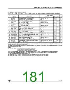
ST90158 - ELECTRICAL CHARACTERISTICS
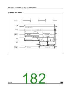
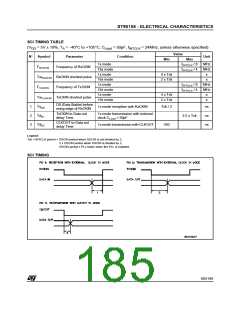
EXTERNAL BUS TIMING TABLE
(V = 5V ± 10%, T = -40°C + 85°C, Cload = 50pF, INTCLK = 16MHz, unless otherwise specified)
DD
N°
A
Value (Note)
Formula
Symbol
TsA (AS)
Parameter
Unit
Min. Max.
1
2
3
4
5
6
7
8
9
Address Set-up Time before AS ↑
Address Hold Time after AS ↑
AS ↑ to Data Available (read)
AS Low Pulse Width
Tck*Wa+TckH-9
TckL-4
23
28
65
27
0
ns
ns
ns
ns
ns
ns
ns
ns
ns
ns
ns
ns
ns
ns
ns
ns
ns
ThAS (A)
TdAS (DR)
TwAS
Tck*(Wd+1)+3
Tck*Wa+TckH-5
0
TdAz (DS)
TwDS
Address Float to DS ↓
DS Low Pulse Width
Tck*Wd+TckH-5
Tck*Wd+TckH+4
7
27
35
7
TdDSR (DR)
ThDR (DS)
TdDS (A)
DS ↓ to Data Valid Delay (read)
Data to DS ↑ Hold Time (read)
DS ↑ to Address Active Delay
DS ↑ to AS ↓ Delay
TckL+11
43
28
15
31
-16
16
29
86
26
10 TdDS (AS)
11 TsR/W (AS)
12 TdDSR (R/W)
13 TdDW (DSW)
14 TsD(DSW)
15 ThDS (DW)
16 TdA (DR)
TckL-4
R/W Set-up Time before AS ↑
DS ↑ to R/W and Address Not Valid Delay
Write Data Valid to DS ↓ Delay
Write Data Set-up before DS ↑
Data Hold Time after DS ↑ (write)
Address Valid to Data Valid Delay (read)
AS ↑ to DS ↓ Delay
Tck*Wa+TckH-17
TckL-1
-16
Tck*Wd+TckH-16
TckL-3
Tck*(Wa+Wd+1)+TckH-7
TckL-6
17 TdAs (DS)
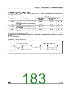
Note: The value in the left hand column shows the formula used to calculate the timing minimum or maximum from the oscillator clock period,
prescale value and number of wait cycles inserted.
The values in the right hand two columns show the timing minimum and maximum for an external clock at 24 MHz divided by 2, prescaler
value of zero and zero wait status.
Legend:
Tck = INTCLK period = OSCIN period when OSCIN is not divided by 2;
2*OSCIN period when OSCIN is divided by 2;
OSCIN period / PLL factor when the PLL is enabled
TckH = INTCLK high pulse width (normally = Tck/2, except when INTCLK = OSCIN, in which case it is OSCIN high pulse width)
TckL = INTCLK low pulse width (normally = Tck/2, except when INTCLK = OSCIN, in which case it is OSCIN low pulse width)
P = clock prescaling value (=PRS; division factor = 1+P)
Wa = wait cycles on AS; = max (P, programmed wait cycles in EMR2, requested wait cycles with WAIT)
Wd = wait cycles on DS; = max (P, programmed wait cycles in WCR, requested wait cycles with WAIT)
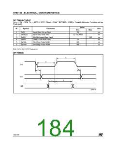
181/199
1

 ETC [ ETC ]