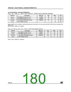
ST90158 - EIGHT-CHANNEL ANALOG TO DIGITAL CONVERTER (A/D)
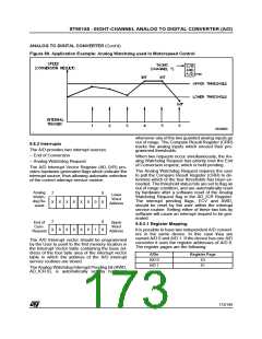
ANALOG TO DIGITAL CONVERTER (Cont’d)
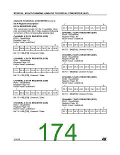
CONTROL LOGIC REGISTER (CLR)
however, the correct procedure is to enable only
one alternate synchronization input at a time.
The Control Logic Register (CLR) manages the
A/D converter logic. Writing to this register will
cause the current conversion to be aborted and
the autoscan logic to be re-initialized.
Note: The effect of either synchronization mode is
to set the START/STOP bit, which is reset by hard-
ware when in SINGLE mode, at the end of each
sequence of conversions.
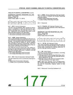
CONTROL LOGIC REGISTER (CLR)
R253 - Read/Write
Register Page: 63
Requirements: The External Synchronisation In-
put must receive a low level pulse longer than an
INTCLK period and, for both External and On-Chip
Event synchronisation, the repetition period must
be greater than the time required for the selected
sequence of conversions.
Reset Value: 0000 0000 (00h)
7
0
EXT
G
CON
T
SC2 SC1 SC0
INTG POW
ST
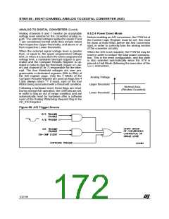
Bit 2 = POW: Power Up/Power Down.
This bit is set and cleared by software.
0: Power down mode: all power-consuming logic is
disabled, thus selecting a low power idle mode.
1: Power up mode: the A/D converter logic and an-
alog circuitry is enabled.
Bit 7:5 = SC[2:0]: Start Conversion Address.
These 3 bits define the starting analog input chan-
nel (Autoscan mode). The first channel addressed
by SC[2:0] is converted, then the channel number
is incremented for the successive conversion, until
channel 7 (111) is converted. When SC2, SC1 and
SC0 are all set, only channel 7 will be converted.
Bit 1 = CONT: Continuous/Single.
0: Single Mode: a single sequence of conversions
is initiated whenever an external (or internal)
trigger occurs, or when the ST bit is set by soft-
ware.
1: Continuous Mode: the first sequence of conver-
sions is started, either by software (by setting
the ST bit), or by hardware (on an internal or ex-
ternal trigger, depending on the setting of the
INTG and EXTG bits); a continuous conversion
sequence is then initiated.
Bit 4 = EXTG: External Trigger Enable.
This bit is set and cleared by software.
0: External trigger disabled.
1: External trigger enabled. Allows a conversion
sequence to be started on the subsequent edge
of the external signal applied to the EXTRG pin
(when enabled as an Alternate Function).
Bit 3 = INTG: Internal Trigger Enable.
This bit is set and cleared by software.
0: Internal trigger disabled.
1: Internal trigger enabled. Allows a conversion se-
quence to be started, synchronized by an inter-
nal signal (On-chip Event signal) from a Multi-
function Timer peripheral.
Bit 0 = ST: Start/Stop.
0: Stop conversion. When the A/D converter is
running in Single Mode, this bit is hardware re-
set at the end of a sequence of conversions.
1: Start a sequence of conversions.
Both External and Internal Trigger inputs are inter-
nally ORed, thus avoiding Hardware conflicts;
176/199
9

 ETC [ ETC ]