ST90158 - EIGHT-CHANNEL ANALOG TO DIGITAL CONVERTER (A/D)
ANALOG TO DIGITAL CONVERTER (Cont’d)
Single and continuous conversion modes are
available. Conversion may be triggered by an ex-
ternal signal or, internally, by the Multifunction
Timer.
In Continuous Mode (CONT = “1”), a continuous
conversion flow is initiated by the start event.
When conversion of channel 7 is complete, con-
version of channel 's' is initiated (where 's' is spec-
ified by the setting of the SC2, SC1 and SC0 bits);
this will continue until the ST bit is reset by soft-
ware. In all cases, an ECV interrupt is issued each
time channel 7 conversion ends.
A Power-Down programmable bit allows the A/D
to be set in low-power idle mode.
The A/D’s Interrupt Unit provides two maskable
channels (Analog Watchdog and End of Conver-
sion) with hardware fixed priority, and up to 7 pro-
grammable priority levels.
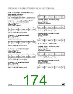
When channel 'i' is converted ('s' <'i' <7), the relat-
ed Data Register is reloaded with the new conver-
sion result and the previous value is lost. The End
of Conversion (ECV) interrupt service routine can
be used to save the current values before a new
conversion sequence (so as to create signal sam-
ple tables in the Register File or in Memory).
CAUTION: A/D INPUT PIN CONFIGURATION
The input Analog channel is selected by using the
I/O pin Alternate Function setting (PXC2, PXC1,
PXC0 = 1,1,1) as described in the I/O ports sec-
tion. The I/O pin configuration of the port connect-
ed to the A/D converter is modified in order to pre-
vent the analog voltage present on the I/O pin from
causing high power dissipation across the input
buffer. Deselected analog channels should also be
maintained in Alternate function configuration for
the same reason.
9.8.2.2 Triggering and Synchronisation
In both modes, conversion may be triggered by in-
ternal or external conditions; externally this may
be tied to EXTRG, as an Alternate Function input
on an I/O port pin, and internally, it may be tied to
INTRG, generated by a Multifunction Timer pe-
ripheral. Both external and internal events can be
separately masked by programming the EXTG/
INTG bits of the Control Logic Register (CLR). The
events are internally ORed, thus avoiding potential
hardware conflicts. However, the correct proce-
dure is to enable only one alternate synchronisa-
tion condition at any time.
9.8.2 Functional Description
9.8.2.1 Operating Modes
Two operating modes are available: Continuous
Mode and Single Mode. To enter one of these
modes it is necessary to program the CONT bit of
the Control Logic Register. Continuous Mode is
selected when CONT is set, while Single Mode is
selected when CONT is reset.
The effect either of these synchronisation modes
is to set the ST bit by hardware. This bit is reset, in
Single Mode only, at the end of each group of con-
versions. In Continuous Mode, all trigger pulses
after the first are ignored.
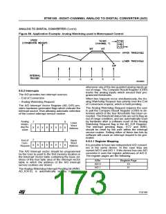
Both modes operate in AUTOSCAN configuration,
allowing sequential conversion of the input chan-
nels. The number of analog inputs to be converted
may be set by software, by setting the number of
the first channel to be converted into the Control
Register (SC2, SC1, SC0 bits). As each conver-
sion is completed, the channel number is automat-
ically incremented, up to channel 7. For example,
if SC2, SC1, SC0 are set to 0,1,1, conversion will
proceed from channel 3 to channel 7, whereas, if
SC2, SC1, SC0 are set to 1,1,1, only channel 7 will
be converted.
The synchronisation sources must be at a logic
low level for at least the duration of one INTCLK
cycle and, in Single Mode, the period between trig-
ger pulses must be greater than the total time re-
quired for a group of conversions. If a trigger oc-
curs when the ST bit is still set, i.e. when conver-
sion is still in progress, it will be ignored.
On devices where two A/D Converters are present
they can be triggered from the same source.
When the ST bit of the Control Logic Register is
set, either by software or by hardware (by an inter-
nal or external synchronisation trigger signal), the
analog inputs are sequentially converted (from the
first selected channel up to channel 7) and the re-
sults are stored in the relevant Data Registers.
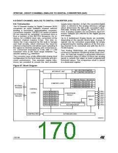
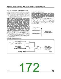
On Chip Event
(Internal trigger)
Converter
External Trigger
EXTRG pin
A/D 0
A/D 1
MFT 0
9.8.2.3 Analog Watchdogs
In Single Mode (CONT = “0”), the ST bit is reset
by hardware following conversion of channel 7; an
End of Conversion (ECV) interrupt request is is-
sued and the A/D waits for a new start event.
Two internal Analog Watchdogs are available for
highly flexible automatic threshold monitoring of
external analog signal levels.
171/199
9

 ETC [ ETC ]