ST90158 - MULTIPROTOCOL SERIAL COMMUNICATIONS INTERFACE (SCI-M)
MULTIPROTOCOL SERIAL COMMUNICATIONS INTERFACE (Cont’d)
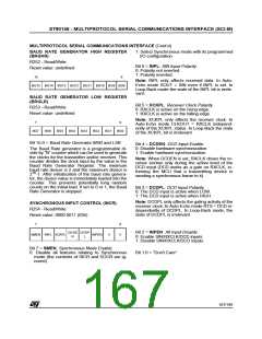
SYNCHRONOUS OUTPUT CONTROL (SOCR)
R255 - Read/Write
Bit 3 = RTSEN: RTS and SDS Output Enable.
0: Disable the RTS and SDS hardware synchroni-
sation.
1: Enable the RTS and SDS hardware synchroni-
sation.
Reset value: 0000 0001 (01h)
7
0
Notes:
– When RTSEN is set, the RTS output becomes
active just before the first active edge of CLK-
OUT and indicates to target device that the MCU
is about to send a synchronous frame; it returns
to its stand-by value just after the last active edge
of CLKOUT (MSB transmitted).
OUTP OUTS OCKP OCKS RTSE RTS OUT
X
L
B
L
B
N
PL
DIS
Bit 7 = OUTPL: SOUT Output Polarity.
0: Polarity not inverted.
1: Polarity inverted.
– When RTSEN is set, the SDS output becomes
active high and indicates to the target device that
the MCU is about to send the first bit of a syn-
chronous frame on the Serial Output Pin
(SOUT); it returns to low level as soon as the
second bit is sent on the Serial Output Pin
(SOUT). In this way a positive pulse is generated
each time that the first bit of a synchronous frame
is present on the Serial Output Pin (SOUT).
Note: OUTPL only affects the data sent by the
transmitter section. In Auto-Echo mode SOUT =
SIN even if OUTPL=1. In Loop-Back mode, the
state of OUTPL is irrelevant.
Bit 6 = OUTSB: SOUT Output Stand-By Level.
0: SOUT stand-by level is HIGH.
1: SOUT stand-by level is LOW.
Bit 2 = RTSPL: RTS Output Polarity.
0: The RTS output is active when LOW.
1: The RTS output is active when HIGH.
Bit 5 = OCKPL: Transmitter Clock Polarity.
0: CLKOUT is active on the rising edge.
1: CLKOUT is active on the falling edge.
Note: RTSPL only affects the RTS activity on the
output pin. In Auto-Echo mode RTS = DCD inde-
pendently from the RTSPL value. In Loop-Back
mode RTSPL value is 'Don't Care'.
Note: OCKPL only affects the transmitter clock. In
Auto-Echo mode CLKOUT = RXCLK independ-
ently of the state of OCKPL. In Loop-Back mode
the state of OCKPL is irrelevant.
Bit 1 = OUTDIS: Disable all outputs.
This feature is available on specific devices only
(see device pin-out description).
When OUTDIS=1, all output pins (if configured in
Alternate Function mode) will be put in High Im-
pedance for networking.
Bit 4 = OCKSB: Transmitter Clock Stand-By Lev-
el.
0: The CLKOUT stand-by level is HIGH.
1: The CLKOUT stand-by level is LOW.
0: SOUT/CLKOUT/enabled
1: SOUT/CLKOUT/RTS put in high impedance
Bit 0 = “Don't Care”
168/199
9

 ETC [ ETC ]